193nm resist with improved post-exposure properties

a post-exposure and resist technology, applied in the microelectronics industry, can solve the problems of inability to obtain finer resolution, inability to produce smaller devices, and inability to use photoresist compositions at the heart of current 248 nm lithographic processes, etc., to achieve good exposure dose latitude, reduce post-exposure bake fluctuations, and high resolution lithographic performance

Inactive Publication Date: 2006-08-08
IBM CORP +1
View PDF14 Cites 25 Cited by
  • Summary
  • Abstract
  • Description
  • Claims
  • Application Information

AI Technical Summary

Benefits of technology

[0006]The invention provides resist compositions which are capable of high resolution lithographic performance with (a) good exposure dose latitude, (b) reduced sensitivity to fluctuations in post-exposure bake and/or (c) reduced line edge roughness. The resists of the invention are pr

Problems solved by technology

The ability to produce smaller devices is limited by the ability of lithographic techniques to reliably resolve smaller features and spacings.
The nature of optics is such that the ability to obtain finer resolution is limited in part by the wavelength of light (or other radiation) used to create the lithographic pattern.
Unfortunately, photoresist compositions at the

Method used


Image

  • 193nm resist with improved post-exposure properties
  • 193nm resist with improved post-exposure properties
  • 193nm resist with improved post-exposure properties

Examples


synthesis example 1

Synthesis of t-butyl-2-methacryloyloxyacetate (C1-tBE) Monomer

[0057]Methacrylic acid (8.06 g, 0.10 mole), t-butyl bromoacetate (19.50 g, 0.10 mole) and 1,8-diazabicyclo[5.4.0]undoc-7-ene, DBU, (15.20 g, 0.10 mole) and 150 ml toluene were combined in a 500 ml 3-neck flask equipped with condenser, nitrogen inlet, thermometer and magnetic stirrer bar. The reaction mixture was stirred at room temperature for one hour. The reaction was continued at 90° C. overnight under a blanket of N2 flow. The mixture was cooled to room temperature and the salt was removed by filtration. The toluene solution was washed with 75 ml saturated NaCl solution and 2×75 ml Dl-water respectively before dried on MgSO4 overnight. The solid was filtered out and the toluene was removed at rotavap. An oily residue was distilled to a final clear liquid at reduced pressure.

synthesis example 2

Synthesis of C1-tBE:NLM Copolymer

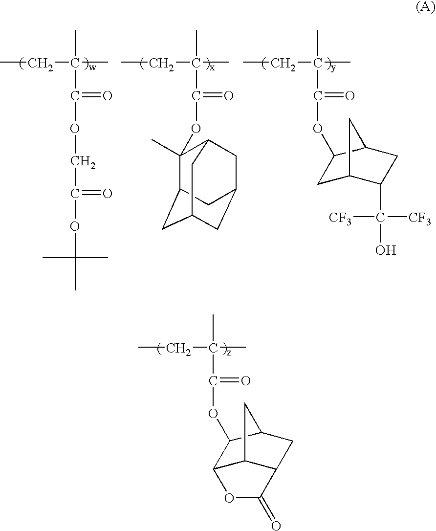
[0058]T-butyl-2-methacryloyloxyacetate, “C1-tBE” (7.5 grams, 0.037 mole), norbornenelactonemethacrylate, “NLM” (12.48 grams, 0.056 mole), 2,2′-azobisisobutylonitrile initiator (0.90 grams, 6.00% total moles), 95 ml of tetrahydrofuran and 50 ml of ethyl acetate were combined in a 250 ml 3-neck round bottom flask equipped with condenser, thermometer, nitrogen inlet and a magnetic stirrer bar. The reaction solution was stirred at room temperature and bubbled with N2 flow for one hour prior turning the heating mantle on. The polymerization was carried out at 70° C. for 14 hours with a blanket of N2 flow. The solution was cooled and added drop wise to 1200 ml stirring methanol. The mixture was stirred overnight before filtration. The copolymer which was collected on the filter was air dried for a few hours before the final drying at vacuum oven at 65° C. The yield was 89%. C13 NMR confirmed the composition of the polymer to be 37:63 (C1-tBE:NLM). GPC indi...

synthesis example 3

Synthesis of C1-tBE:NLM:MAdMA Terpolymer

[0059]T-butyl-2-methacryloyloxyacetate, “C1-tBE” (1.38 grams, 0.0074 mole), methyladamantylmethacrylate, “MAdMA” (1.76 grams, 0.0074 mole), norbornenelactonemethacrylate, “NLM” (5.88 grams, 0.0224 mole), 2,2′-azobisisobutylonitrile initiator (0.40 gram, 6.75% total of moles), 40 ml of tetrahydrofuran, and 20 ml of ethyl acetate were combined in a 250 ml 3-neck, round bottom flask equipped with condenser, thermometer, nitrogen inlet and magnetic stirrer bar. The mixture was stirred at room temperature and bubbled with N2 flow for 45 minutes prior turning the heating mantle on. The reaction was conducted for 14 hours at 70° C. with a blanket of N2 flow. Then the reaction solution was cooled to room temperature and added drop wise to 500 ml of stirring methanol. The resulting slurry was stirred overnight before filtration. The solid was collected from the filter and air dried for five hours. The final drying was carried out in a vacuum oven at 65...


PUM

PropertyMeasurementUnit
Nanoscale particle sizeaaaaaaaaaa
Weightaaaaaaaaaa
Solubility (mass)aaaaaaaaaa

Abstract

Acid-catalyzed positive resist compositions which are imageable with 193 nm radiation and/or possibly other radiation and are developable to form resist structures of improved development characteristics and improved etch resistance are enabled by the use of resist compositions containing imaging polymer component comprising an acid-sensitive polymer having a monomeric unit with a pendant group containing a remote acid labile moiety.

Description

BACKGROUND OF THE INVENTION[0001]In the microelectronics industry as well as in other industries involving construction of microscopic structures (e.g. micromachines, magnetoresistive heads, etc.), there is a continued desire to reduce the size of structural features. In the microelectronics industry, the desire is to reduce the size of microelectronic devices and / or to provide greater amount of circuitry for a given chip size.[0002]The ability to produce smaller devices is limited by the ability of lithographic techniques to reliably resolve smaller features and spacings. The nature of optics is such that the ability to obtain finer resolution is limited in part by the wavelength of light (or other radiation) used to create the lithographic pattern. Thus, there has been a continual trend toward use of shorter light wavelengths for lithographic processes. Recently, the trend has been to move from so-called I-line radiation (350 nm) to 248 nm radiation. For future reductions in size,...

Claims


Application Information

Patent Timeline
IPC IPC(8): G03C1/73G03F7/039G03F7/20G03F7/30G03F7/36G03F7/38
CPCG03F7/0392G03F7/0395Y10S430/115Y10S430/108Y10S430/111Y10S430/106
Inventor KHOJASTEH, MAHMOUD H.CHEN, KUANG-JUNGVARANASI, PUSHKARA RAONISHIMURA, YUKIOKOBAYASHI, EIICHI
Owner IBM CORP
Why Eureka
Try Eureka