
Nonvolatile semiconductor memory device, charge injection method thereof and electronic apparatus

a semiconductor memory and non-volatile technology, applied in the direction of digital storage, transistors, instruments, etc., can solve the problems of long writing time and erasing time, hard for the fg type to achieve a low voltage, and the efficiency of generating hot carriers is declining, so as to achieve low voltage operation and high data rewriting speed

Inactive Publication Date: 2006-08-15
SONY CORP
View PDF4 Cites 8 Cited by
  • Summary
  • Abstract
  • Description
  • Claims
  • Application Information

AI Technical Summary

Benefits of technology

[0023]An object of the present invention is to improve a hot-carrier generation efficiency even when an operation voltage is low in a charge injection method of applying different voltages to a source region and a drain region.
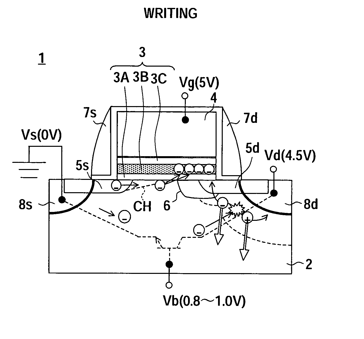
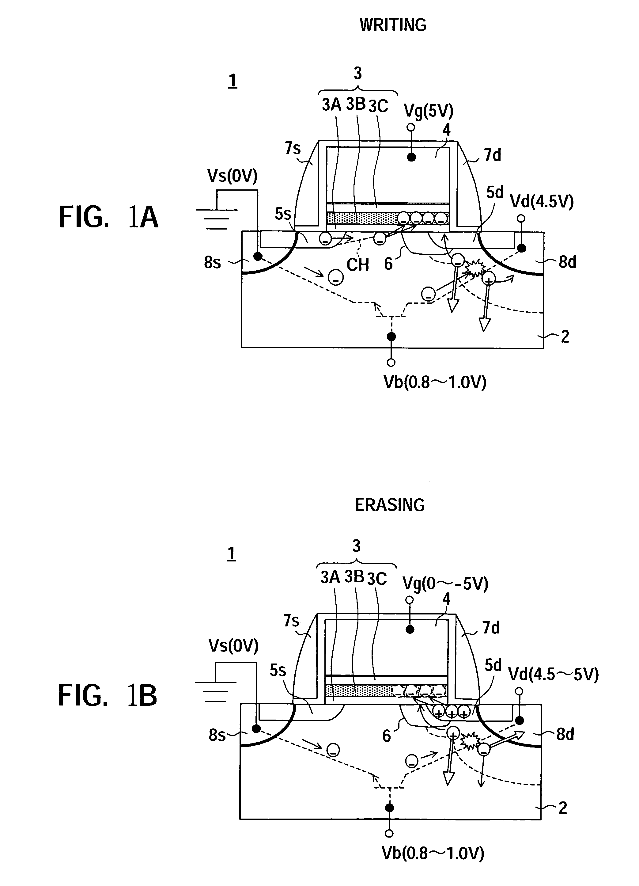
[0031]Therefore, other than charges injected to the charge storage layer the same as in the conventional case of not applied with a body bias voltage, charges generated as a result that a bipolar transistor is turned on as explained above are injected to a stacked insulation film. Accordingly, an efficiency of injecting charges is improved, and a predetermined threshold voltage change is brought even by a low operation voltage, so that the charge injection time becomes short. Also, when assuming that the charge injection time is the same, charge injection at a lower operation voltage becomes possible.
[0033]According to the electronic apparatus according to the present invention, even in the case where only a nonvolatile semiconductor memory device configured to be not provided with a function of generating a body bias voltage, as far as a terminal for supplying a voltage to the body region is provided, the charge injection method of the present invention can be applied by connecting the nonvolatile semiconductor memory device to a supply circuit of the body bias voltage incorporated in the same electronic apparatus. Consequently, it is possible to realize an electronic apparatus capable of attaining a high data rewriting speed or a low voltage operation.

Problems solved by technology

Furthermore, it is hard for the FG type to attain a low voltage due to the reason that the gate oxide film (tunnel oxide film) cannot be made very thin or a coupling capacitance of the gate and the channel is large, etc.
This point is a common problem of the FG type and the MONOS type.
In this case, the above-explained charge injection method of applying different voltages to a source region and a drain region, as in the CHE injection and the HH injection, has a disadvantage of bringing a decline of the efficiency of generating hot carriers due to the low operation voltage, and a writing time and an erasing time become long.

Method used


Image

  • Nonvolatile semiconductor memory device, charge injection method thereof and electronic apparatus
  • Nonvolatile semiconductor memory device, charge injection method thereof and electronic apparatus
  • Nonvolatile semiconductor memory device, charge injection method thereof and electronic apparatus

Examples


Embodiment Construction

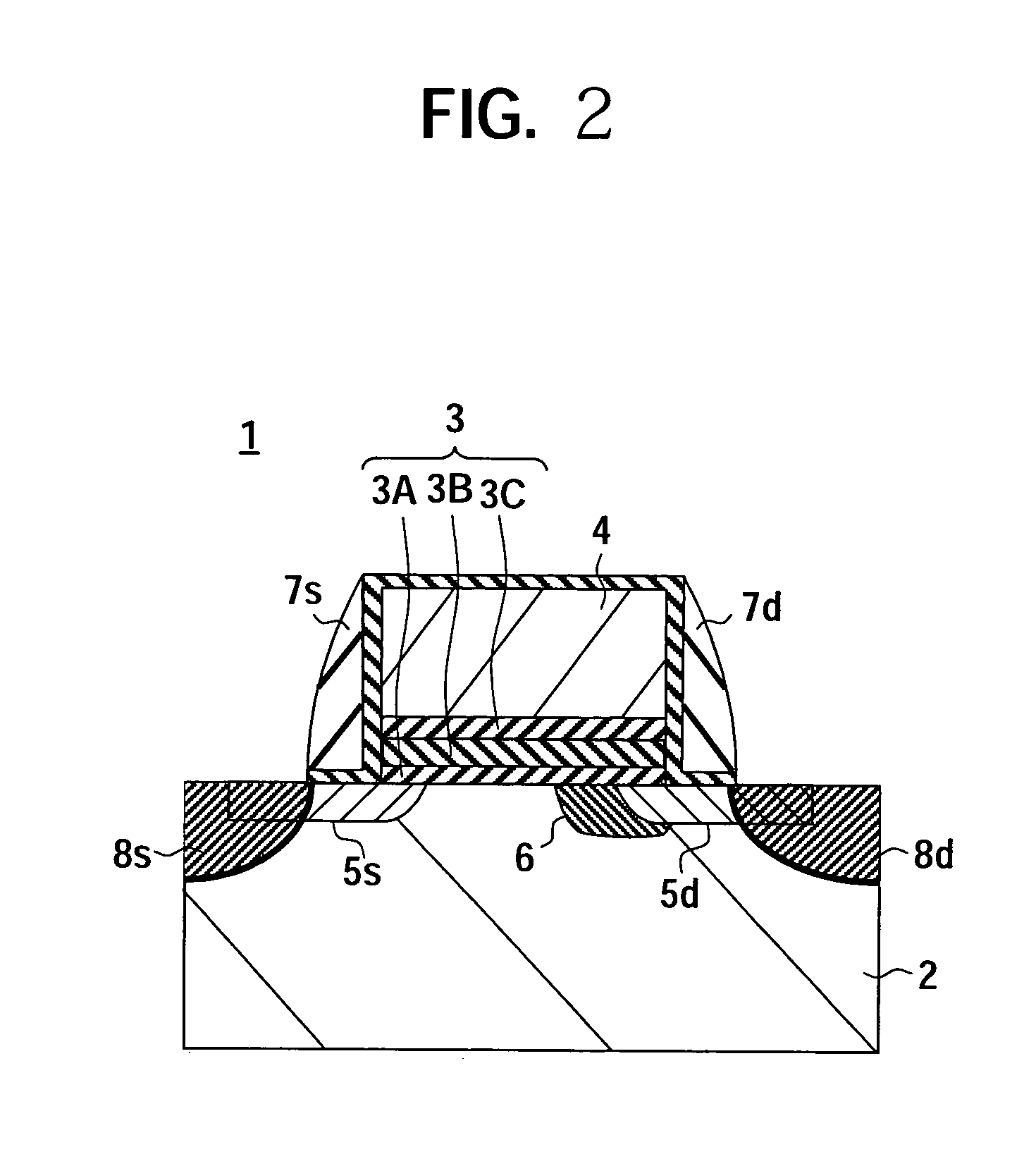
[0040]Below, embodiments of the present invention will be explained with reference to the drawings by taking an example of a flash EEPROM having an N-channel type MONOS transistor.

[0041]Note that the present invention can be applied to memory transistors having a gate electrode configuration, except for the MONOS type. For example, the present invention can be widely applied to memory transistors having a gate configuration, such as an FG type, a so-called MNOS (metal-nitride-oxide-semiconductor) type, and a nanocrystal type wherein conductive fine particles are buried in a stacked insulation film. Also, the present invention is not limited to the N-channel type and can be applied to a P-channel type. In that case, by setting conductive types having inverse polarities to an impurity and channel and switching polarities of voltages of a source region and a drain region as will be explained below, the explanation below may be applied analogically.

[0042]FIG. 2 is a sectional view of a ...


PUM

PropertyMeasurementUnit
voltageaaaaaaaaaa
ground voltage GNDaaaaaaaaaa
gate voltage Vgaaaaaaaaaa

Abstract

A charge injection method for improving the efficiency of generating hot carriers, wherein, for example, electrons are injected at writing and holes are injected at erasing to a charge storage layer of a memory transistor. A positive voltage is applied to the drain region by using a voltage of the source region as a reference, and a voltage having a polarity in accordance with charges to be injected is applied to a gate electrode. A voltage having a voltage value between a source voltage and a drain voltage for turning on a diode made by an N-type source region and a P-type body region is applied to the body region. Then a parasitic bipolar transistor turns on, and, consequently, impact ionization arises on the drain side and an injection charge amount increases.

Description

BACKGROUND OF THE INVENTION[0001]1. Field of the Invention[0002]The present invention relates to a charge injection method of a nonvolatile semiconductor memory device (flash EEPROM) by applying different voltages to a source region and a drain region, a nonvolatile semiconductor memory and an electronic apparatus incorporating the same.[0003]2. Description of the Related Art[0004]A flash EEPROM as a kind of nonvolatile memory stores data in accordance with a charge storage state of a charge storage layer. As a flash EEPROM, there is a device having a gate structure wherein charges accumulated in a charge storage layer are made by conductive polysilicon (FG type) and having a gate structure wherein conductivity of the charge storage layer is extremely low as in a typical MONOS (metal-oxide-nitride-oxide-semiconductor) type. In the FG type, electrons are injected, for example, from a whole surface of a channel to tunnel through the gate oxide film, so that the electrons are accumulat...

Claims


Application Information

Patent Timeline
Patent Type & Authority Patents(United States)
IPC IPC(8): G11C11/34G11C16/04H01L21/8247H01L27/115H01L29/76H01L29/788H01L29/792
CPCG11C16/10H01L21/28282H01L29/872H01L27/11568H01L29/0891H01L27/11565H01L29/40117H10B43/10H10B43/30
Inventor MORI, HIDEKI
Owner SONY CORP
Learn More