Transistor with shallow germanium implantation region in channel

a technology of germanium implantation and transistor, which is applied in the direction of transistors, crystal growth processes, chemistry apparatus and processes, etc., can solve the problems of deteriorating mobility, affecting the performance of devices, and impractical use of thin oxides in many device applications, so as to improve the gate dielectric quality, reduce the thermal budget, and increase the mobility of holes and electrons

Active Publication Date: 2006-08-22
INFINEON TECH AG
View PDF30 Cites 20 Cited by
  • Summary
  • Abstract
  • Description
  • Claims
  • Application Information

AI Technical Summary

Benefits of technology

[0013]These and other problems are generally solved or circumvented, and technical advantages are generally achieved, by preferred embodiments of the present invention, which includes a transistor and method of fabrication thereof, having a channel region with a very shallow high concentration of germanium implanted therein. A low-temperature anneal process is used to re-crystallize the germanium implantation region in the channel region and eliminate defects or damage caused by the implantation process. A gate dielectric material is formed over the channel region, before or after the low-temperature anneal process, and a gate is formed over the high-k gate dielectric. Source and drain regions are formed by implanting dopants and using a low-temperature anneal process to drive in the dopants. Due to the presence of a high concentration of germanium at the top surface of the channel, and because of the low-temperature anneal processes used in accordance with embodiments of the present invention, the effective oxide thickness of the gate dielectric is kept to a minimum, resulting in a thinner effective gate dielectric (or oxide) thickness. The implanted germanium also increases the mobility of the channel region due to the strain in the channel region caused by the size misfit between silicon atoms and germanium atoms. For example, germanium atoms are larger than silicon atoms, so when germanium is introduced into a silicon atomic lattice structure, the larger germanium atoms create stress in the atomic structure in the channel region.
[0017]Advantages of preferred embodiments of the present invention include providing a transistor design and manufacturing method thereof, wherein the total anneal temperature for the transistor manufacturing process flow is reduced, reducing the thermal budget and improving the gate dielectric quality. Because of the presence of germanium in the workpiece, and because the anneal process to re-crystallize the amorphous germanium-containing region comprises a low temperature, the effective gate oxide thickness is kept to a minimum. The germanium in the channel region increases the mobility of holes and electrons in the channel region, resulting in a transistor device with a faster response time and increased drive current.

Problems solved by technology

However, as devices are scaled down in size, using silicon dioxide for a gate dielectric becomes a problem because of gate leakage current, which can degrade device performance.
However, the resulting gate leakage current makes the use of such thin oxides impractical in many device applications where low standby power consumption is required.
However, device performance using high k dielectric materials tends to suffer from trapped charge in the dielectric layer, which deteriorates the mobility, making the drive current lower than in transistors having silicon dioxide gate oxides, thus reducing the speed and performance of transistors having high k gate dielectric materials.
Another problem with the prior art structure 100 is that the high temperature anneal processes used to form the source S and drain D tend to degrade the dielectric constant of the high k gate dielectric 108.
Another challenge in the scaling of transistors is increasing the mobility in the channel region, which increases the speed of the device.

Method used


Image

  • Transistor with shallow germanium implantation region in channel
  • Transistor with shallow germanium implantation region in channel
  • Transistor with shallow germanium implantation region in channel

Examples


Embodiment Construction

[0024]The making and using of the presently preferred embodiments are discussed in detail below. It should be appreciated, however, that the present invention provides many applicable inventive concepts that can be embodied in a wide variety of specific contexts. The specific embodiments discussed are merely illustrative of specific ways to make and use the invention, and do not limit the scope of the invention.

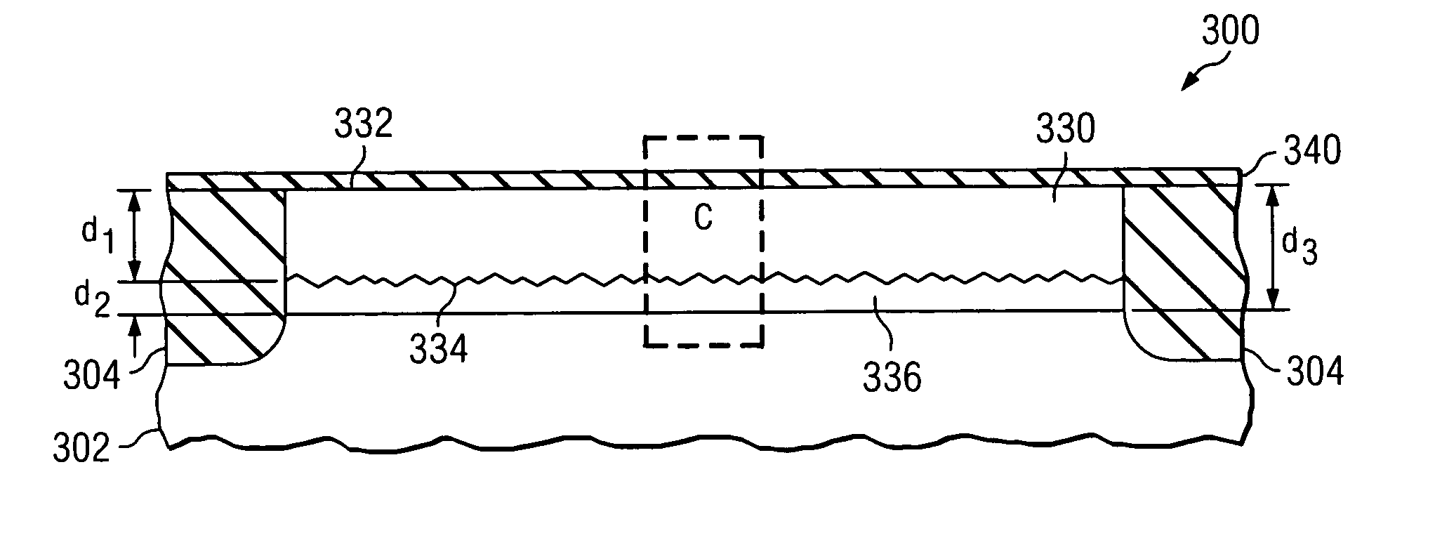
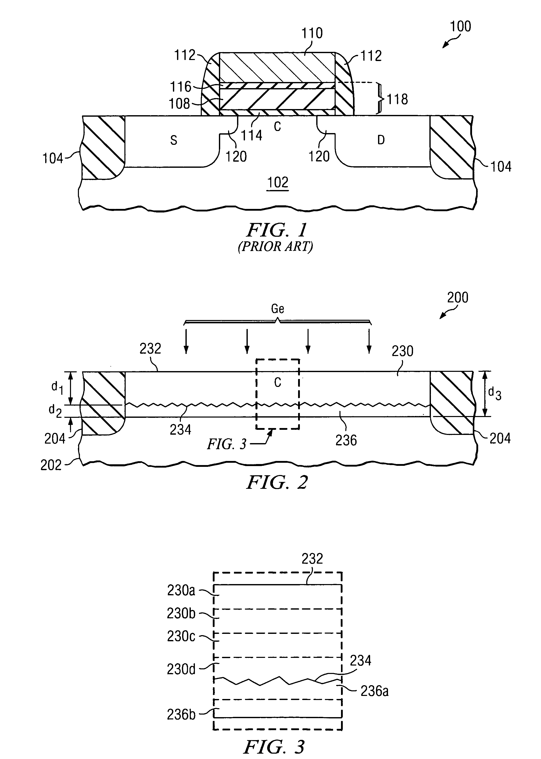
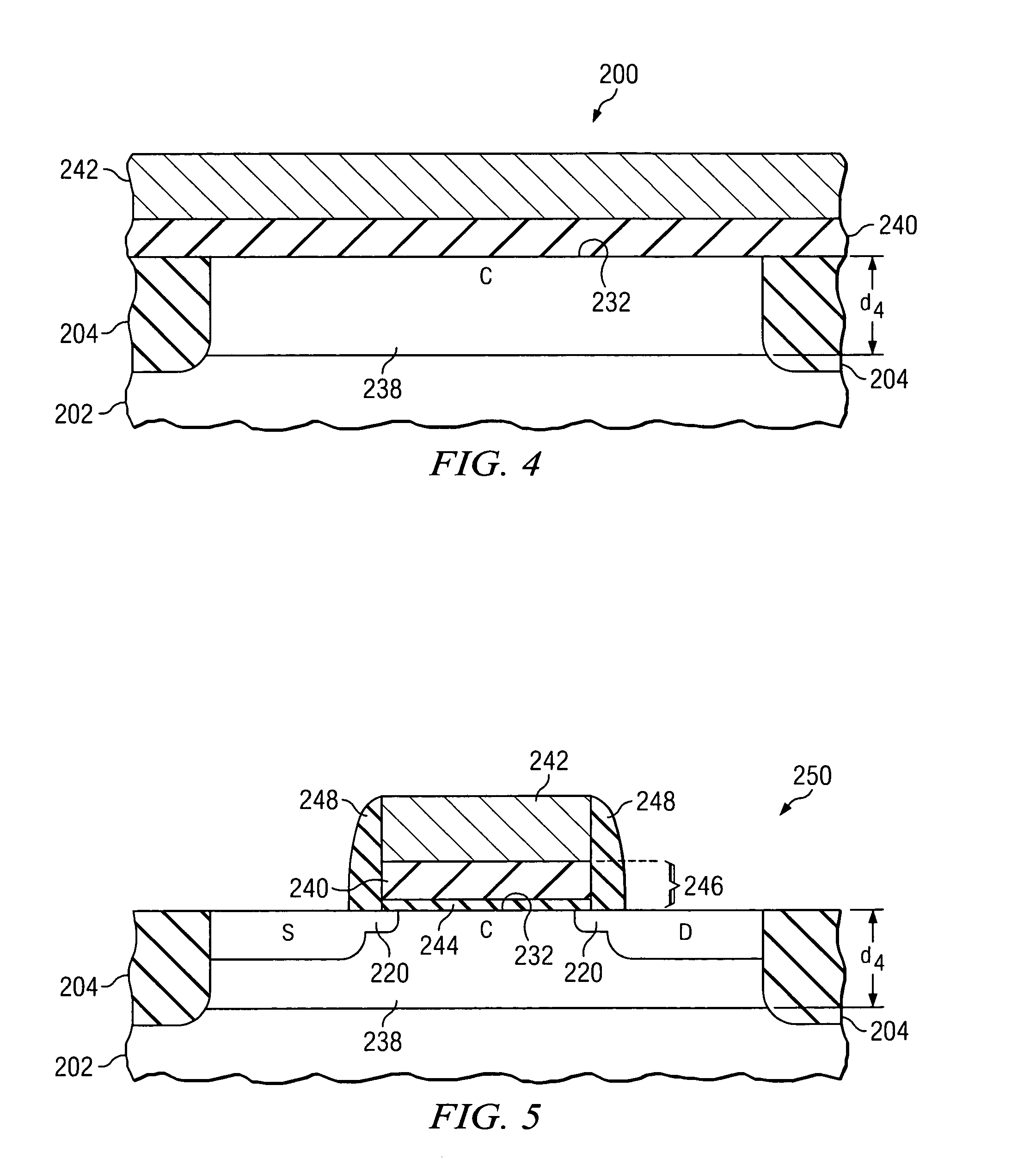
[0025]The present invention will be described with respect to preferred embodiments in a specific context, namely a transistor formed on a semiconductor device. The invention may also be applied, however, to MOSFETs or other transistor devices, including p channel metal oxide semiconductor (PMOS) transistors, n channel metal oxide semiconductor (NMOS) transistors, and / or complimentary metal oxide semiconductor (CMOS) devices, as examples. Only one transistor is shown in each of the figures; however, there may be many other transistors and devices formed in the manufacturing p...


PUM

PropertyMeasurementUnit
dielectric constantaaaaaaaaaa
temperatureaaaaaaaaaa

Abstract

A method of manufacturing a transistor and a structure thereof, wherein a very shallow region having a high dopant concentration of germanium is implanted into a channel region of a transistor at a low energy level, forming an amorphous germanium implantation region in a top surface of the workpiece, and forming a crystalline germanium implantation region beneath the amorphous germanium implantation region. The workpiece is annealed using a low-temperature anneal to convert the amorphous germanium region to a crystalline state while preventing a substantial amount of diffusion of germanium further into the workpiece, also removing damage to the workpiece caused by the implantation process. The resulting structure includes a crystalline germanium implantation region at the top surface of a channel, comprising a depth below the top surface of the workpiece of about 120 Å or less. The transistor has increased mobility and a reduced effective oxide thickness (EOT).

Description

CROSS-REFERENCE TO RELATED APPLICATIONS[0001]This patent application relates to the following co-pending and commonly assigned patent applications: Ser. No. 10 / 748,995, filed on Dec. 30, 2003, entitled, “Transistor with Silicon and Carbon Layer in the Channel Region;” and Ser. No. 10 / 771,075, filed on Feb. 3, 2004, entitled, “Transistor with Doped Gate Dielectric,” which applications are hereby incorporated herein by reference.TECHNICAL FIELD[0002]The present invention relates generally to semiconductor devices, and more particularly to a method of fabricating a transistor and a structure thereof.BACKGROUND[0003]Semiconductor devices are used in a variety of electronic applications, such as personal computers, cell phones, digital cameras, and other electronic equipment, as examples. A transistor is an element that is utilized extensively in semiconductor devices. There may be millions of transistors on a single integrated circuit (IC), for example. A common type of transistor used ...

Claims


Application Information

Patent Timeline
Patent Type & Authority Patents(United States)
IPC IPC(8): H01L21/265C30B1/00H01L21/00H01L21/20H01L21/28H01L21/3205H01L21/324H01L21/336H01L21/36H01L21/4763H01L21/84H01L29/06H01L29/51H01L29/78H01L31/0328H01L31/0336H01L31/072H01L31/109
CPCH01L21/28185H01L21/28194H01L21/324H01L29/517H01L21/26506H01L21/28088Y10S438/933H01L29/513H01L29/6659H01L21/28273H01L29/40114H01L21/2658
Inventor LI, HONG-JYH
Owner INFINEON TECH AG
Why Eureka
Try Eureka