Photoelectric conversion device

Inactive Publication Date: 2006-08-22
SEMICON ENERGY LAB CO LTD +1
View PDF38 Cites 65 Cited by
  • Summary
  • Abstract
  • Description
  • Claims
  • Application Information

AI Technical Summary

Benefits of technology

[0028]The conventional method utilizing the prior art roll-to-roll scheme as typically shown in FIG. 9 makes use of the dark portion close to the cathode or anode for plasma processing. On the other hand, the present invention makes positive use of a positive column produced by a plasma discharge, thus improving the productivity of the plasma processing. In FIG. 8, the flexible substrate is supplied substantially perpendicular to the surfaces of the discharge electrodes 202 and 203. The direction of supply is not limited to this direction. Similar advantages can be obtained by supplying the substrate parallel or at an angle to the surfaces of the electrodes as long as the total length of the substrate staying in the plasma processing region is longer.
[0029]Where a coating is formed by plasma processing, the surface of the substrate is preferably parallel to the direction of gravity. In particular, when a coating is formed, dust and fla

Problems solved by technology

Of photoelectric conversion devices using these flexible substrates, photoelectric conversion devices employing substrates made of organic materials have attracted attention because of their cost, characteristics, and workability.
Substrates having poor thermal resistance such as the aforementioned flexible substrates made of organic materials are not sufficiently resistant to heat compared with substrates made of other materials.
Consequently, excessive heat is applied to only a part of the organic material of the flexible substrate.
If the leads are bonded to the electrodes of the photoelectric conversion device at a temperature at which no thermal deformation takes place, then a sufficient bonding strength cannot be obtained.
Under th

Method used


Image

  • Photoelectric conversion device
  • Photoelectric conversion device
  • Photoelectric conversion device

Examples


Example

EXAMPLE 1

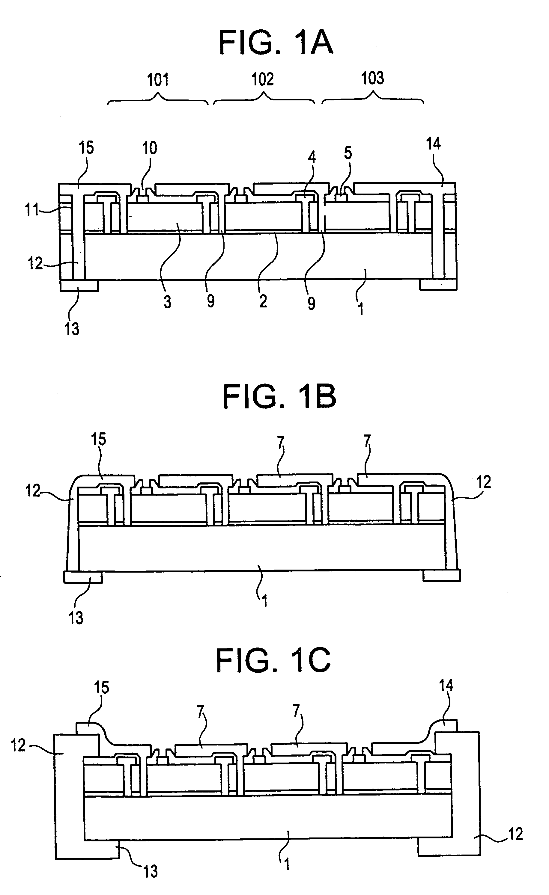
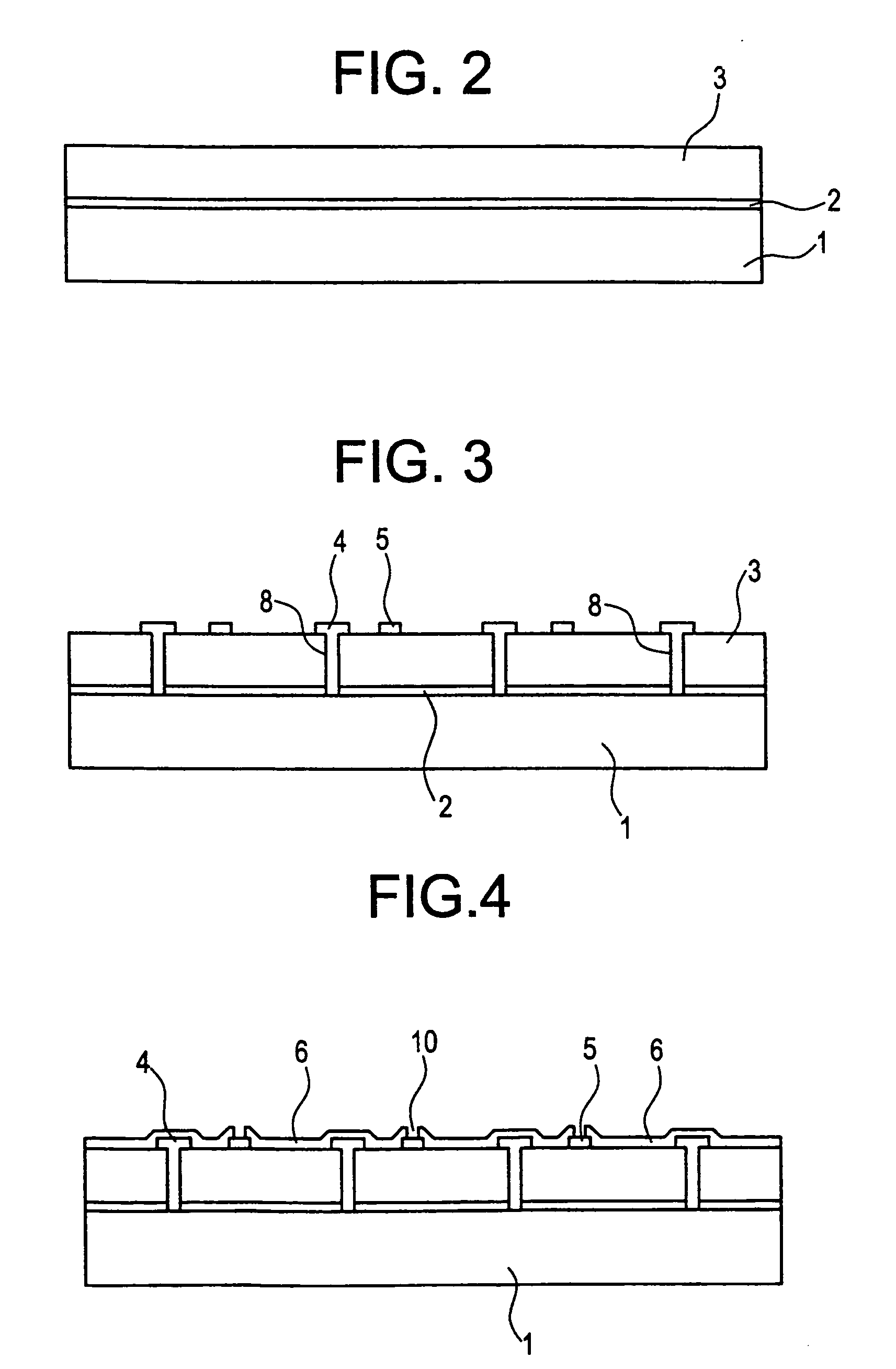
[0042]FIG. 1(A) shows an integrated photoelectric conversion device according to the invention. This photoelectric conversion device is composed of a flexible substrate 1 made of plastic film, a first electrode 2, a PIN-type photoelectric conversion layer 3, second electrodes 6, 7, and insulators 4, 5. The insulators 4 and 5 consist of epoxy resin.

[0043]The photoelectric conversion device has photoelectric elements 101, 102, and 103. The second electrode 7 of the photoelectric element 101 is electrically connected with the first electrode 2 of the photoelectric element 102 by a connector portion 9. The device is provided with a first groove 8 to isolate the first electrode of the first photoelectric element from the photoelectric conversion layer of the second photoelectric element 102. The second electrodes 6 of these elements 101 and 102 are insulated from each other by a groove 10 formed by a laser scriber.

[0044]Simultaneously with formation of the second electrode 7 for...

Example

EXAMPLE 2

[0086]This example of photoelectric conversion device takes a form as illustrated in FIG. 1(B). In this structure, connector portions 12 used to connect the second electrodes 7 with output terminals 13 located on the rear surface of the substrate are formed at the end surfaces of the substrate. Other manufacturing steps are similar to the corresponding steps of Example 1 but the laser illumination steps for piercing the substrate is dispensed with.

[0087]Since the end surfaces of the substrate are used as the connector portions 12, the output terminals 13 are adhesively bonded to the rear surface of the substrate so as to protrude from the substrate. This example yields the same advantages as Example 1 but is able to reduce the number of manufacturing steps. Unlike Example 1, the connector portions 12 do not have limited size. Therefore, the reliability of connection and the production yield can be improved further.

Example

EXAMPLE 3

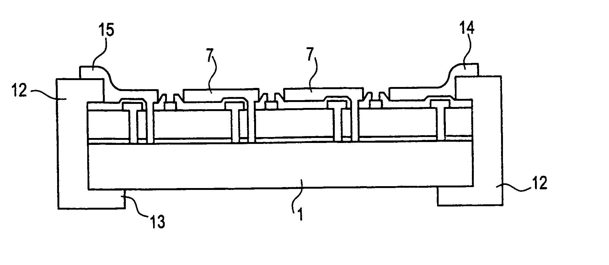
[0088]This example of photoelectric conversion device takes a form as illustrated in FIG. 1(C). In this structure, connector portions 12 used to connect the second electrodes 7 with output terminals 13 located on the rear surface of the substrate are formed on the end surfaces of the substrate. Unlike Example 2, the connector portions 12 are not made of the same material as the second electrodes 7. Rather, the connector portions 12 are made of the same material as the output terminals 13 formed on the rear surface of the substrate. These connector portions 12 made of a metal are located on opposite sides of the substrate and clamp it therebetween. Other manufacturing steps are similar to the corresponding steps of Example 1 but the laser illumination step for piercing the substrate is dispensed with.

[0089]Each metal clamp acting as one connector portion 12 and also as one output terminal 13 takes a U-shaped form with respect to the cross section of the photoelectric convers...


PUM


Abstract

A photoelectric conversion device taking the form of a thin film and having a substrate exhibiting poor thermal resistance. The device prevents thermal deformation which would normally be caused by local application of excessive heat to the substrate. The device has output terminals permitting the output from the device to be taken out. The output terminals are formed on the surface of the substrate opposite to the photoelectric conversion device. The device further includes electrical connector portions for electrically connecting the electrodes of the device with the output terminals. The present invention also provides a method of treating a substrate having poor thermal resistance with a plasma with a high throughput. The substrate is continuously supplied into a reaction chamber and treated with a plasma. This supply operation is carried out in such a way that the total length of the substrate existing in a plasma processing region formed by electrodes is longer than the length of the electrodes.

Description

[0001]This is a divisional of application Ser. No. 09 / 149,289 filed on Sep. 9, 1998, now U.S. Pat. No. 6,720,576, which is a divisional of application Ser. No. 08 / 554,241 filed on Nov. 8, 1995, now U.S. Pat. No. 5,821,597, which is a divisional of application Ser. No. 08 / 118,672 filed on Sep. 9, 1993, now abandoned.FIELD OF THE INVENTION[0002]The present invention relates to a photoelectric conversion device having a novel structure and, more particularly, to a photoelectric conversion device employing a flexible substrate having poor thermal resistance. Also, the invention relates to processing of this flexible substrate such as formation of a coating on the substrate and, more particularly, to a method of treating the flexible substrate with a plasma when a solar cell or the like is fabricated by the use of a flexible organic film instead of a solid substrate.BACKGROUND OF THE INVENTION[0003]The market has required smaller, thinner, and even lighter electronic and electric parts. ...

Claims


Application Information

Patent Timeline
IPC IPC(8): H01L31/0203H01L27/142H01L31/0392H01L31/20
CPCH01L31/03921H01L31/202H01L31/046H01L31/206Y02E10/50H01L31/0463Y02P70/50
Inventor NAKAJIMA, SETSUOARAI, YASUYUKISHINOHARA, HISATOABE, MASAYOSHI
Owner SEMICON ENERGY LAB CO LTD
Why Eureka
Try Eureka