Nanotube-based vacuum devices

a vacuum device and nanotube technology, applied in the field of nanotube-based vacuum devices, can solve the problems of relatively high threshold voltage, complex fabrication technique, and capacitance of electron-gates, and achieve the effect of reducing the threshold voltage for electron emission

Inactive Publication Date: 2006-09-05
ITUS
View PDF2 Cites 31 Cited by
  • Summary
  • Abstract
  • Description
  • Claims
  • Application Information

AI Technical Summary

Benefits of technology

[0015]The presented below device structures have in common one important element, namely, the nanotube as an electron source, from which electrons move in vacuum to the positively biased anode electrode. The nanotubes are placed or grown on the cathode metal electrode in close proximity to the gate electrode (or anode electrode if the diode is under consideration) to minimize the threshold voltage for the electron emission.
[0016]In the devices discussed below, according to the present invention, the nanotubes are treated individually, so that a single nanotube is sufficient for the device operation. The important feature in the majority of presented device designs is extremely low input and output capacitances to maximize the device speed (see below). The nanotubes are placed or grown on the cathode electrode, while all other elements are made using modern planar batch fabrication IC technology. This is an important factor for future possibilities of mass production of nanotube-based, hybrid, high-speed vacuum electronic devices and circuits. Furthermore, the growth of the nanotubes in predetermined positions using e-beam lithography, provides the entire device fabrication cycle for industrial production. It is also important that the number of steps for the device fabrication is very limited: one needs 3–4 photolithography masks versus 10–11 masks for the Si-based transistor, while the most appropriate substrate for vacuum devices is a piece of glass. These factors make the manufacturing cost for these devices significantly lower than that for the Si-based electronics.
[0017]The unique property of the proposed hybrid devices is extremely sharp dependence of the electron field emission current on the cathode-anode voltage, which originates from the mechanism of electron field induced tunneling into vacuum which is determined by the well known Fouler-Nordheim I-V dependence. This dependence is much sharper than typical exponential curve of the forward bias semiconductor diode at room temperature, ˜exp(eV / kT). This yields much higher rectification ratio than in semiconductor diodes. Taking into account small, less then micron, anode-cathode distances, one can obtain the threshold for the current emission from the nanotube within a fraction of a volt, and thus create the most efficient and the fastest diode, far superior than typical Si p-n diode or any Schottky diode. The same field emission mechanism provides extremely high transconductance for the proposed active elements, such as triodes (see below).
[0018]It is also important that the anode can be moved away from the cathode and gate electrodes without compromising the device speed due to high electron velocity in vacuum. This provides an opportunity to increase the anode (output) voltage to the values which are not attainable in Si-based devices.
[0019]Planar device technology used for the proposed devices allows realization of a simple approach for making vacuum chamber as a small cavity over the device structure using conventional methods of dielectric coatings, which significantly reduces the device production cost, see R. S. Mullar et al U.S. Pat. No. 5,493,177. Furthermore, in the structures where the cathode-anode distance is made shorter than 1 μm, and therefore comparable with electron mean free path in the normal atmosphere, there is no need for vacuum. It is preferable in this case to fill the cavity with an inert gas, to minimize possible oxidation and degradation of the nanotube tip.
[0021]The proposed vacuum device technology is entirely compatible with Si IC technology. All fabrication processes needed for the nanotube vacuum electronics can be produced on the Si substrate. The combination of both techniques can be very helpful in increasing the speed of the Si-based circuitry, as well as raising the output voltages.

Problems solved by technology

The problem of vacuum electronics is related to a reliable and compact electron source, to replace the commonly used hot filament cathode.
However, such a design has fundamental problems of a high input (emitter-gate) capacitance and relatively high threshold voltage for electron emission.
In addition, this structure is three-dimensional and requires complex technique for its fabrication, not compatible with modem planar semiconductor IC technology.
This significantly reduces the nanotube efficiency.
This implies that a single nanotube is sufficient for the device operation, and the nanotube array is used only to proportionally increase the emission current.3. In all the cited patents, the controlling gate electrode serves to extract electrons from the nanotube, which inevitably creates undesirable effect of current leakage to the gate electrode.
The subsequent technological operations after nanotube placement are known to adversely affect the nanotube efficiency as an electron source.
The nanotube placement is followed by several processing steps, which may degrade the nanotube performance.

Method used


Image

  • Nanotube-based vacuum devices
  • Nanotube-based vacuum devices
  • Nanotube-based vacuum devices

Examples


Embodiment Construction

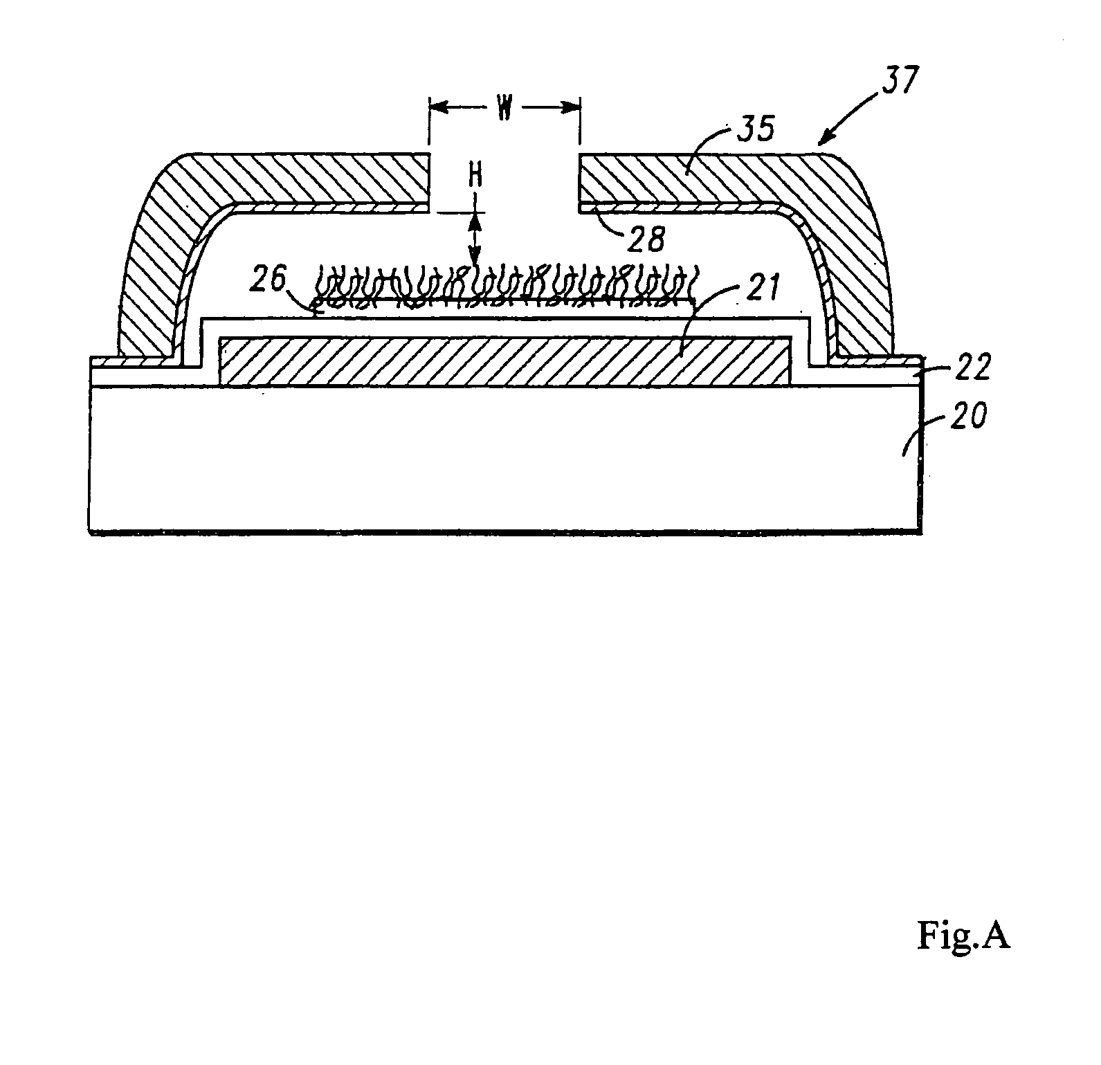
[0042]The majority of the devices presented, has in common an important feature, namely, extremely short distance between the nanotube tip and the gate electrode (or anode electrode, if the diode is considered) to minimize the control voltage for the device operation. At the same time, the device design allows for low input capacitance. For that purpose, the cathode and the gate electrodes are laterally shifted from each other to avoid their overlap, while their planes are separated from each other by the thickness of the dielectric layer. Using self-align method of deposition of the gate electrode (or anode electrode for a diode) next to the cathode electrode, one obtains the cathode-gate (anode) distance essentially controlled by the thickness of the dielectric film, which can easily made within a fraction of a micron.

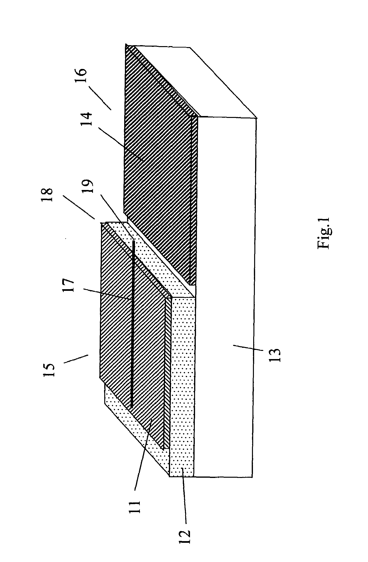
[0043]FIG. 1 illustrates the preferred embodiment of the Diode 1. The conducting film 11 of the cathode electrode 15 is placed on the dielectric film 12 deposited on...


PUM


Abstract

New, hybrid vacuum electronic devices are proposed, in which the electrons are extracted from the nanotube into vacuum. Each nanotube is either placed on the cathode electrode individually or grown normally to the cathode plane. Arrays of the nanotubes are also considered to multiply the output current. Two- and three-terminal device configurations are discussed. In all the cases considered, the device designs are such that both input and output capacitances are extremely low, while the efficiency of the electron extraction into vacuum is very high, so that the estimated operational frequencies are expected to be in a tera-hertz range. New vacuum triode structure with ballistic electron propagation along the nanotube is also considered.

Description

[0001]This is a continuation-in-part of application Ser. No. 10 / 764,168, filed Jan. 26, 2004.FIELD OF THE INVENTION[0002]This invention relates to new devices for vacuum electronics. In particular, it utilizes nanotubes as cold emission electron sources in the two- and three- terminal devices.BACKGROUND OF THE INVENTION[0003]The nanotubes are viewed to be a new approach in electronics with potential to drastically extent the frequency range of modem electronic devices. Such unique properties as quantization of the electron spectrum, ballistic electron propagation along the tube, current densities as high as 109 A / cm2, existence of the semiconductor phase, possibilities for n- and p- doping and fabrication of transistors, make the nanotubes a great candidate for future high-speed device technology.[0004]Another very important application of the nanotubes is cold cathodes, which are based on low threshold electron field emission due to strong electrical field focusing at the nanotube ...

Claims


Application Information

Patent Timeline
Patent Type & Authority Patents(United States)
IPC IPC(8): H01L35/24H01J19/24H01J21/04H01J21/10
CPCB82Y10/00H01J19/24H01J21/04H01J21/105Y10S977/876H01J2201/30469Y10S977/938
Inventor KASTALSKY, ALEXANDERSHOKHOR, SERGEY
Owner ITUS
Why Eureka
Try Eureka