Selective epitaxial growth for tunable channel thickness

a technology of tunable channel and epitaxial growth, which is applied in the field of selective ep, can solve the problems of body introduction of dynamic instabilities, inability to charge and discharge the body, and inability to fully deplete devices, so as to increase the thickness of the exposed underlying semiconductor layer and increase the thickness of the semiconductor layer

Active Publication Date: 2006-09-12
GLOBALFOUNDRIES US INC
View PDF2 Cites 102 Cited by
  • Summary
  • Abstract
  • Description
  • Claims
  • Application Information

AI Technical Summary

Benefits of technology

[0009]An advantage of the present invention is a method of fabricating a semiconductor device comprising different types of transistors with individually tuned channel thicknesses.
[0010]Additional advantages and other aspects and features of the present invention will be set forth in the description which follows and in part will become apparent to those having ordinary skill in the art upon examination of the following or may be learned from the practice of the present invention. The advantages of the present invention may be realized and obtained as particularly pointed out in the appended claims.
[0011]According to the present invention, the foregoing and other advantages are obtained in part by a method of manufacturing a semiconductor device, the method comprising: forming a plurality of isolation regions in a semiconductor layer to define active regions; exposing a particular active region; conducting selective epitaxial growth to selectively increase the thickness of the semiconductor layer in the particular active region; forming a gate dielectric layer on the active regions; and forming a gate electrode on the gate dielectric layer in the active regions.
[0012]Embodiments include forming a plurality of trench isolation regions in the semiconductor layer of an SOI substrate, wherein the semiconductor layer comprises Si. After forming the shallow trench isolation regions which define a plurality of active regions, one or more active regions are selected for tailoring the channel thickness of the transistor to be formed therein, e.g., a P-MOS, N-MOS, a wide transistor or a narrow transistor, partially depleted transistor or a fully depleted transistor. After a particular active region is selected, the nitride stop layer and pad oxide layer are removed exposing the underlying semiconductor layer in the particular active region. Selective epitaxial growth is then implemented to selectively increase the thickness of the exposed underlying semiconductor layer in the particular active region. Subsequently, the nitride stop layers and pad oxide layers are removed in the other active regions, thermal oxidation is conducted to form gate oxide layers and gate electrodes are formed on the gate oxide layers. The transistors are completed by implementing ion implantation in a conventional manner.
[0013]In other embodiments of the present invention, the semiconductor layer of the SOI substrate comprises Si—Ge. In these embodiments, a protective layer of silicon is deposited after selective epitaxial growth, as by thermal chemical vapor deposition (CVD). The deposited layer of Si protects the epitaxially grown layer during acid treatment to remove the nitride stop layer.
[0014]Additional advantages and aspects of the present invention will become readily apparent to those skilled in the art from the following detailed description, wherein embodiments of the present invention are shown and described, simply by way of illustration of the best mode contemplated for practicing the present invention. As will be described, the present invention is capable of other and different embodiments, and its several details are susceptible of modification in various obvious respects, all without departing from the spirit of the present invention. Accordingly, the drawings and description are to be regarded as illustrative in nature, and not as limitative.

Problems solved by technology

However, the floating body can introduce dynamic instabilities in the operation of such a transistor.
The fully depleted devices do not have a neutral region in the channel and thus do not allow for charging and discharging of the body corresponding to the change in threshold voltage.
Additionally, the fully depleted devices do not show hysterisis effect.

Method used


Image

  • Selective epitaxial growth for tunable channel thickness
  • Selective epitaxial growth for tunable channel thickness
  • Selective epitaxial growth for tunable channel thickness

Examples


Embodiment Construction

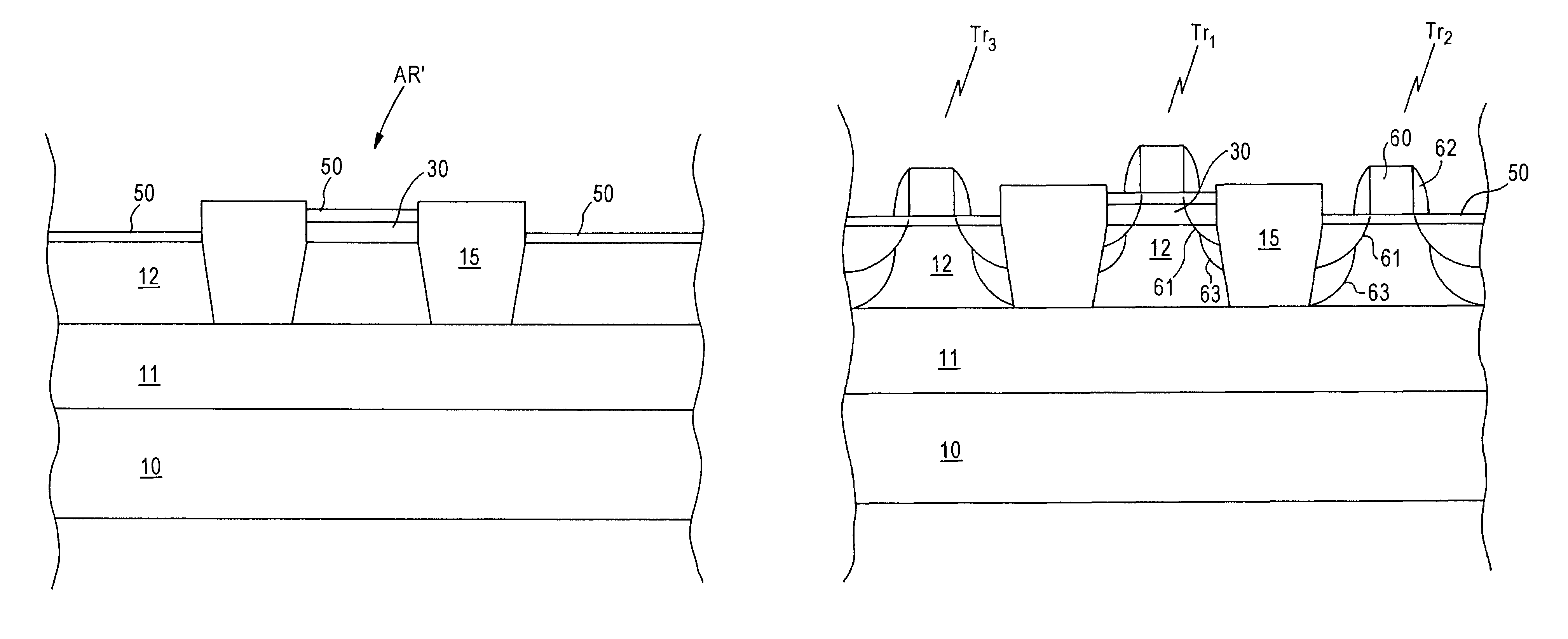
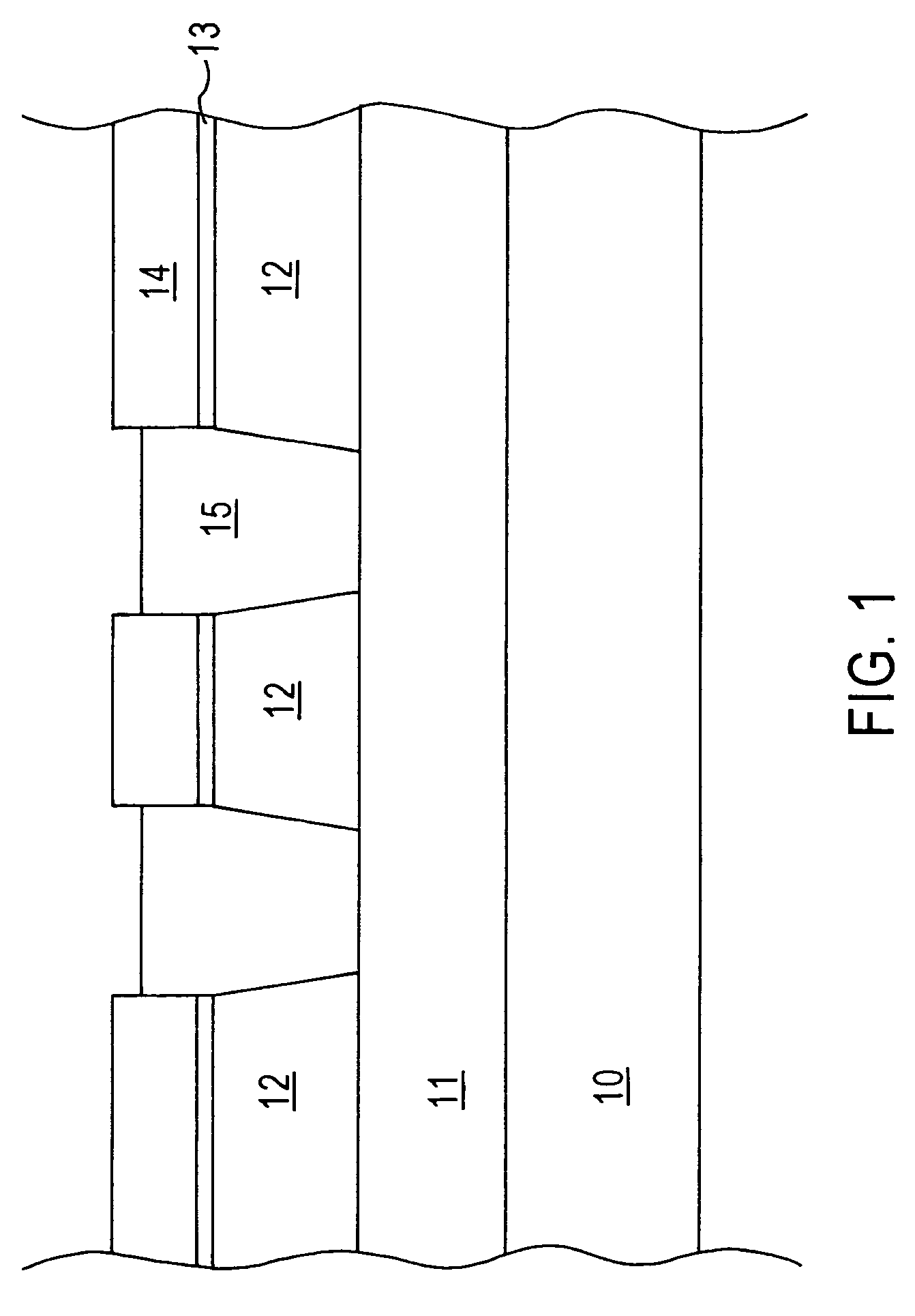
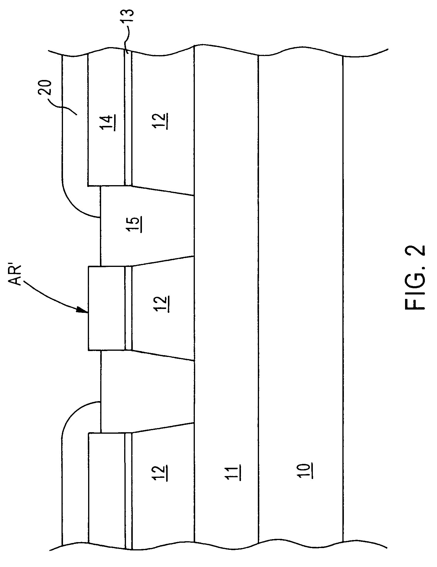
[0018]The present invention addresses and solves the problem of optimizing the performance characteristics of a semiconductor device comprising different types of transistors for a particular implementation. Semiconductor devices typically comprise various different types of transistors designed to perform certain functions. The present invention provides efficient methodology enabling the transistors to be selectively tuned with a desired channel thickness depending on its desired characteristics for the particular implementation. In this way the overall operating speed of the device is increased with improved accuracy and precision in an efficient, cost effective manner.

[0019]In accordance with embodiments of the present invention, designated active regions wherein transistors are to be formed which desirably have a thicker channel than other transistors are subjected to selective epitaxial growth in order to increase the channel thickness vis-à-vis the channels of other transisto...


PUM


Abstract

Gate electrodes with selectively tuned channel thicknesses are formed by selective epitaxial growth. Embodiments include forming shallow trench isolation regions in an SOI substrate, selectively removing the nitride stop layer and pad oxide layer in an exposed particular active region, and implementing selective epitaxial growth to increase the thickness of the semiconductor layer in the particular active region. Subsequently, the remaining nitride stop and pad oxide layers in other active regions are removed, gate dielectric layers formed, as by thermal oxidation, and the transistors completed.

Description

FIELD OF THE INVENTION[0001]The present invention relates to the fabrication of micro-miniaturized semiconductor devices having increased operating speed. The present invention is particularly applicable in fabricating semiconductor devices comprising different types of transistors with tunable channel thicknesses.BACKGROUND OF THE INVENTION[0002]The relentless pursuit of miniaturized semiconductor devices continues to challenge the limitations of conventional semiconductor materials and fabrication techniques. Conventional semiconductor devices typically comprise a plurality of active devices in or on a common semiconductor substrate, e.g., CMOS devices comprising at least a pair of PMOS and NMOS transistors in spaced adjacency. Current technology utilizes crystalline semiconductor wafers as substrates, such as a lightly p-doped epitaxial (“epi”) layer of silicon (Si) grown on a heavily-doped, crystalline Si Substrate. The low resistance of the heavily-doped substrate is necessary ...

Claims


Application Information

Patent Timeline
Patent Type & Authority Patents(United States)
IPC IPC(8): H01L21/302H01L21/8238
CPCH01L21/823807H01L27/1203H01L21/84
Inventor DAKSHINA-MURTHY, SRIKANTESWARABONSER, DOUGLASVAN MEER, HANSBROWN, DAVID
Owner GLOBALFOUNDRIES US INC
Why Eureka
Try Eureka