Wireless communication semiconductor integrated circuit device and mobile communication system

a technology of integrated circuits and semiconductors, applied in the direction of oscillation generators, pulse automatic control, instruments, etc., can solve the problems of increasing the thermal noise of resistive elements, increasing the chip size, and expanding the memory capacity, so as to reduce the control sensitivity and shorten the time

Inactive Publication Date: 2006-10-17
RENESAS TECH CORP
View PDF4 Cites 41 Cited by
  • Summary
  • Abstract
  • Description
  • Claims
  • Application Information

AI Technical Summary

Benefits of technology

[0008]In order to solve this deficiency, the inventors of this invention examined the following: increasing the oscillation frequency bands of the VCO further more, decreasing the ratio of an oscillation frequency variation against a control voltage variation in each frequency band, thereby reducing the control sensitivity of the VCO, thus making it difficult for the influence of the thermal noises to appear on the output of the VCO, even if the resistances of the resistive elements constituting the loop filter are increased.
[0018]Further, by incorporating the loop filter into one chip, the total number of components becomes decreased, and the downsizing becomes possible. Because of decreased power consumption, it is possible to implement a mobile telephone and other wireless communication systems that can elongate the maximum call time and the maximum standby time.

Problems solved by technology

However, to increase the resistances will increase the thermal noises by the resistive elements.
In such a system as disclosed in the Patent Reference 1 that measures the actual frequencies on all the frequency bands in advance and stores the measurement results in a memory in order to determine a usable oscillation frequency band in the VCO capable of switching the oscillation frequency bands, there is a possibility of causing an increase of the chip size, because further increasing the frequency bands of the VCO elongates the measuring time further more to increase the power consumption, and it also requires expanding the capacity of the memory for storing the measurement results.
Therefore, in the case the VCO has a large number of frequency bands, there is a possibility that the system to determine the usable frequency band as proposed in the Patent Reference 1 is not appropriate.

Method used


Image

  • Wireless communication semiconductor integrated circuit device and mobile communication system
  • Wireless communication semiconductor integrated circuit device and mobile communication system
  • Wireless communication semiconductor integrated circuit device and mobile communication system

Examples


Embodiment Construction

[0027]The preferred embodiments will now be described with reference to the accompanying drawings.

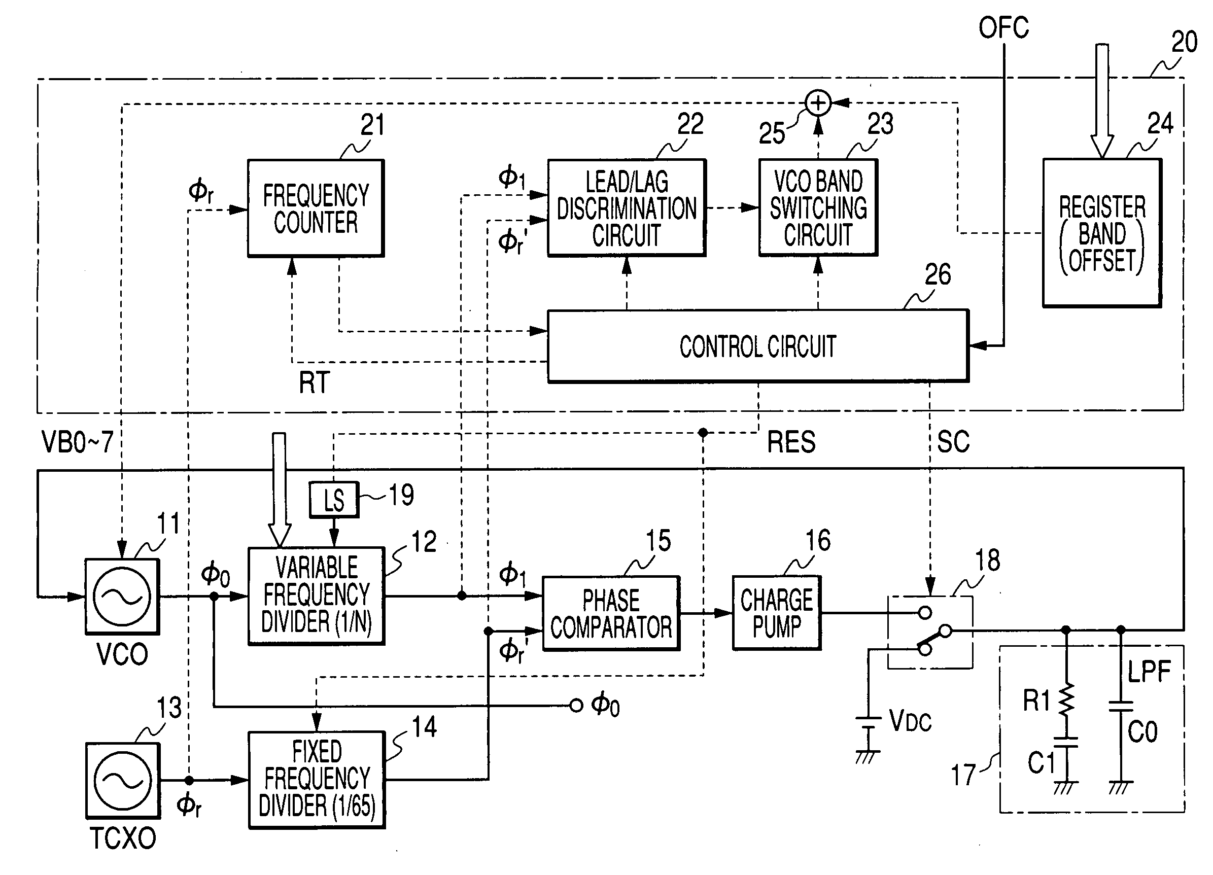
[0028]FIG. 1 illustrates one embodiment of the PLL circuit relating to the invention, which contains the function that automatically selects a usable band of the VCO based on the externally set frequency information.

[0029]The PLL circuit of this embodiment includes a voltage controlled oscillator (VCO) 11, a variable frequency divider 12 that divides the frequency of an oscillation signal φ0 from the VCO into 1 / N the frequency, a fixed frequency divider 14 that divides the frequency of 26 MHz, for example, of a reference oscillation signal φr from a reference frequency oscillator 13 to generate the reference oscillation signal φr, a phase comparator 15 that detects the phase difference between a signal φ1 acquired by the variable frequency divider 12 dividing the frequency of the oscillation signal φ0 and a signal φr′ acquired by the fixed frequency divider 14 dividing the frequency of ...


PUM


Abstract

An RF IC in which a PLL circuit including a loop filter is incorporated into a semiconductor chip is achieved without increasing power consumption or chip size. The RF IC includes a VCO capable of switching oscillation frequency bands, a variable frequency divider, a phase comparator, and a loop filter, which are contained in the PLL loop. A discrimination circuit discriminates a lead or lag in a phase of an output signal from the variable frequency divider against a reference signal and an automatic band selecting circuit generates a signal for switching the frequency bands of the VCO based on output from the discrimination circuit. While switching the frequency bands of the VCO by means of bisection algorithm, the RF IC detects an optimum frequency band, and adds offset to it to determine a final usable frequency band.

Description

CROSS REFERENCE TO RELATED APPLICATION[0001]The present application claims priority from the Japanese patent application No. 2003-337000 filed on Sep. 29, 2003, the content of which is hereby incorporated by reference into this application.BACKGROUND OF THE INVENTION[0002]The present invention relates to a technique effective in application to a semiconductor integrated circuit device incorporating a PLL (phase locked loop) circuit, specifically to a technique effective in use for a radio frequency semiconductor integrated circuit device incorporating a PLL circuit that generates a predetermined frequency oscillation signal synthesized with a reception signal or a transmission signal for a wireless communication, and a mobile communication system containing the same.[0003]In a wireless communication system such as a mobile telephone, a radio frequency semiconductor integrated circuit device (hereunder, referred to as an RF IC) is used which incorporates a PLL circuit including an os...

Claims


Application Information

Patent Timeline
Patent Type & Authority Patents(United States)
IPC IPC(8): H03L7/18H03L7/10H03L7/00H03L7/089H03L7/099H03L7/187H03L7/199
CPCH03L7/099H03L7/10H03L7/199H03L7/0891H03L7/104
Inventor UOZUMI, TOSHIYAOSAWA, HIROTAKASHINBO, JIROYAMAMOTO, SATORU
Owner RENESAS TECH CORP
Why Eureka
Try Eureka