Semiconductor laser device

a laser device and semiconductor technology, applied in the direction of lasers, semiconductor devices, semiconductor lasers, etc., can solve the problems of reducing the aspect ratio, kink level and other aspects, and disadvantageous configuration for the transfer of heat to the radiating body, so as to improve the transfer of heat, enhance reliability, and lessen the end-face degradation

Inactive Publication Date: 2006-10-31
MITSUBISHI ELECTRIC CORP
View PDF4 Cites 24 Cited by
  • Summary
  • Abstract
  • Description
  • Claims
  • Application Information

AI Technical Summary

Benefits of technology

[0011]The present invention has been made to solve the foregoing problems. A first object of the present invention is to provide a semiconductor laser device which reduces the angle of expansion of a vertical beam to lessen end-face degradation at a high-power operation and improves the transfer of heat to a radiating body to thereby enhance reliability at the high-power operation.
[0013]Accordingly, in the semiconductor laser device according to the present invention, an effective refractive index of a semiconductor layer lying on the radiating body side with respect to an active layer is set lower than that of a semiconductor layer lying on the non-radiating body side with respect to the active layer to thereby expand a light intensity distribution to the non-radiating body side with respect to the active layer to reduce an aspect ratio, and the angle of expansion of a vertical beam is reduced to ensure a satisfactory high-power operation. Further, a thermal resistance of the semiconductor layer disposed on the radiating body side with respect to the active layer is set smaller than that of the semiconductor layer disposed on the non-radiating body side with respect to the active layer to thereby enable satisfactory transfer of heat to the radiating body side.
[0014]Hence, the semiconductor laser device according to the present invention can be configured which enables a high-power operation and makes it easy to transfer heat produced with the high-power operation to a radiator. By extension, a semiconductor laser can be provided whose high-power operation is high in reliability.
[0016]Accordingly, in the semiconductor laser device according to the present invention, an effective refractive index determined based on the first semiconductor layer and the third semiconductor layer is lower than an effective refractive index determined based on the fourth semiconductor layer and the second semiconductor layer to thereby expand a light intensity distribution to the fourth semiconductor layer to reduce an aspect ratio, and the angle of expansion of a vertical beam is reduced to ensure a satisfactory high-power operation. Further, a thermal resistance determined based on the first semiconductor layer and the third semiconductor layer is smaller than a thermal resistance determined based on the fourth semiconductor layer and the second semiconductor layer, to thereby enable satisfactory transfer of heat to the radiating body side.
[0017]Hence, the semiconductor laser device according to the present invention can be configured which enables a high-power operation and makes it easy to transfer heat produced with the high-power operation to a radiator. By extension, a semiconductor laser can be provided whose high-power operation is high in reliability.

Problems solved by technology

However, a semiconductor laser device with a high-power operation encounters an important problem of how to effectively conduct heat generated in a laser chip to a radiator or radiating body.
Therefore, a thermal conductivity distribution of materials constituting a semiconductor laser for conducting the generated heat to the radiating body, as well as a mere improvement in kink level and reduction in aspect ratio become an important problem.
Therefore, according to how to take or determine refractive indices of a cladding layer disposed on the radiating body side and a cladding layer disposed on the non-radiating body side, this might be a configuration disadvantageous to the transfer of heat to the radiating body.

Method used


Image

  • Semiconductor laser device
  • Semiconductor laser device
  • Semiconductor laser device

Examples


first embodiment

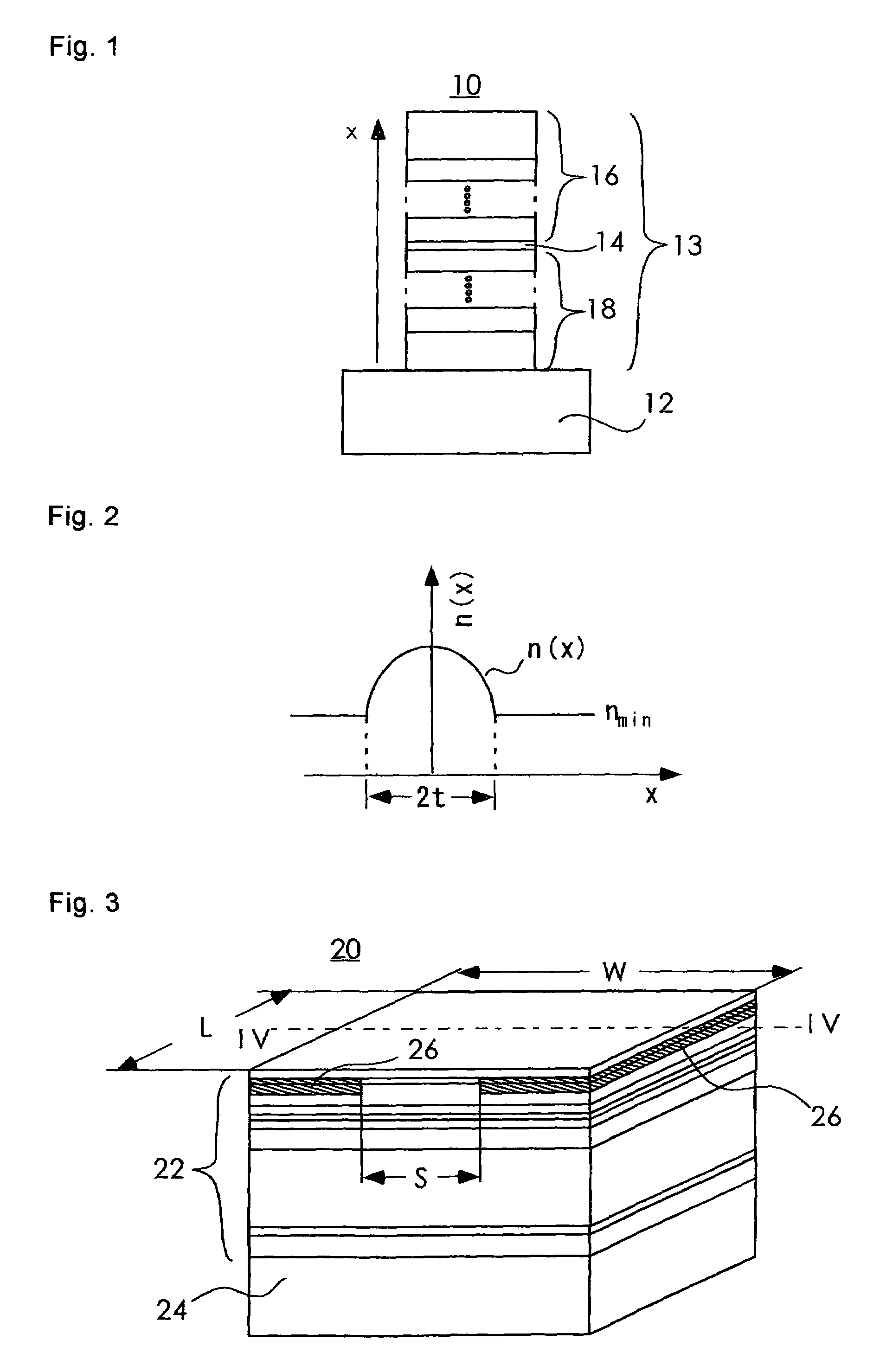
[0042]FIG. 1 is a typical diagram of a semiconductor laser device according to one embodiment of the present invention. FIG. 2 is a typical diagram showing a refractive index distribution of semiconductor layers of the semiconductor laser device according to the present invention.

[0043]The first embodiment will explain a basic configuration containing even embodiments from a second embodiment.

[0044]In FIG. 1, the semiconductor laser device 10 comprises a heat sink 12 used as a radiator or radiating body, and a semiconductor laser element 13 disposed on the heat sink 12. The semiconductor laser element 13 is constituted of a semiconductor layer 16 and a semiconductor layer 18 laminated on each other with an active layer 14 interposed therebetween. The semiconductor layer 16 is provided on the side opposite to the heat sink 12 with respect to the active layer 14 and the semiconductor layer 18 is provided on the heat sink 12 side with respect to the active layer 14, respectively.

[0045]...

second embodiment

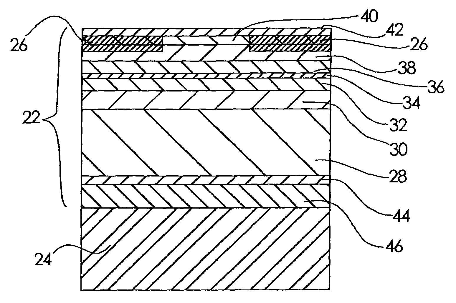
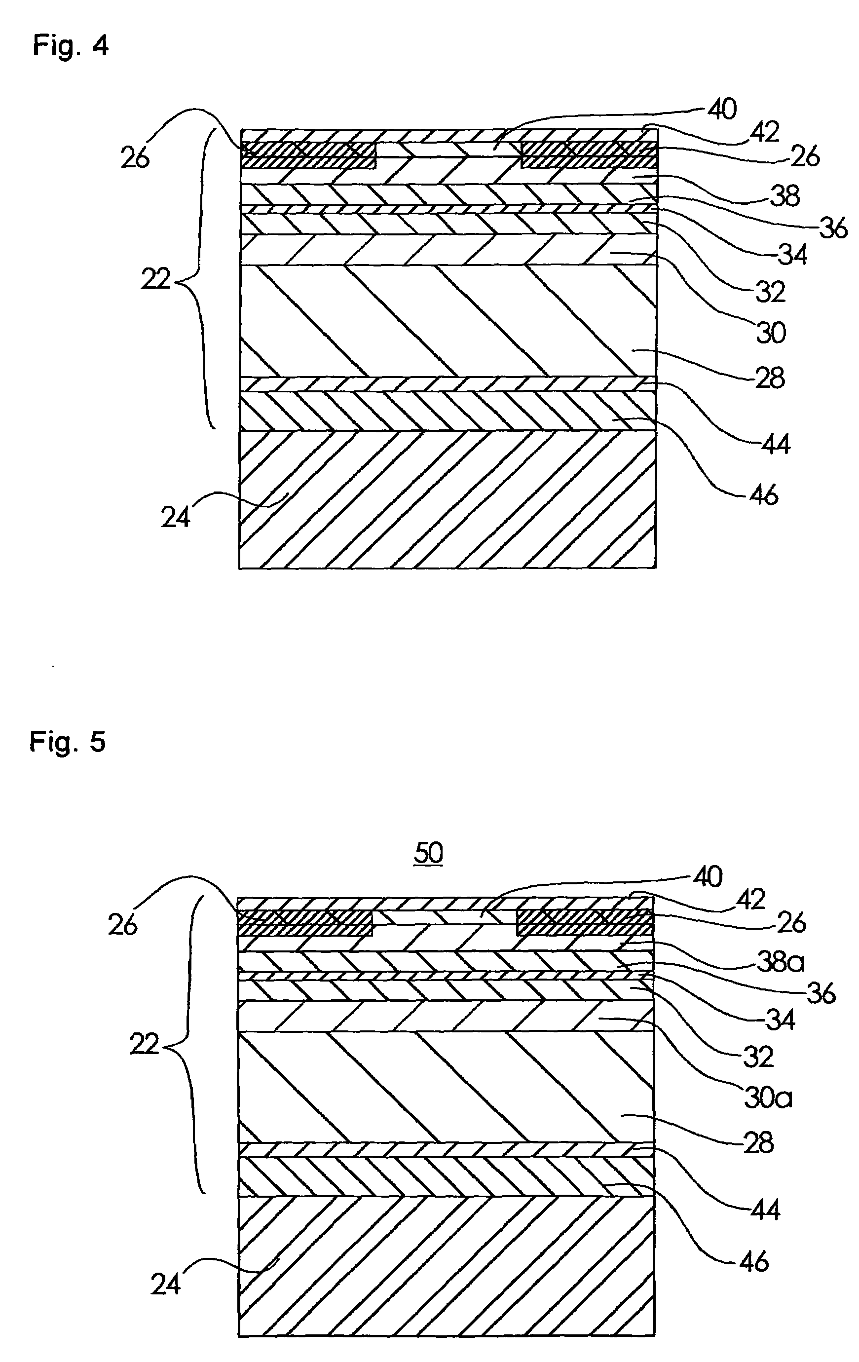
[0064]FIG. 3 is a perspective view of a semiconductor laser device according to one embodiment of the present invention. FIG. 4 is a cross-sectional view of the semiconductor laser device as viewed in a cross-section taken along line IV—IV of FIG. 3.

[0065]The second through fifth embodiments will explain, as an example, a semiconductor laser device used as an excitation light source of a solid state laser whose oscillation wavelength lies in the neighborhood of 810 nm, e.g., a YAG laser used for metal welding and cutting-off.

[0066]In FIG. 3, the semiconductor laser device 20 is formed of a semiconductor laser element 22 and a CuW heat sink 24 used as a radiating body or radiator. Hatched portions are proton injection regions 26 for current restriction. The hatching shown in FIG. 3 does not show a cross-section. A portion pinched between the proton injection regions 26 is a stripe corresponding to a region in which a current flows. The width of the stripe is expressed in S. In the se...

modification 1

[0086]FIG. 5 is a cross-sectional view of a modification of the semiconductor laser device according to one embodiment of the present invention. Since FIG. 5 is also basically identical in configuration to FIG. 2, the position of a section of FIG. 5 also corresponds to the section taken along line IV—IV of FIG. 3. Incidentally, the same reference numerals in the respective drawings indicate the same or equivalent ones.

[0087]The semiconductor laser device 50 shown in FIG. 5 is different from the semiconductor laser device 20 in that an n-AlGaAs cladding layer 30a is configured with its Al composition ratio as x=0.90 and its thickness as t=0.4 μm, and a p-AlGaAs cladding layer 38a is configured with its Al composition ratio as x=0.55 and its thickness as t=2.0 μm. The semiconductor laser device 50 is identical in other configuration to the semiconductor laser device 20.

[0088]Even in the case of the semiconductor laser device 50 as well as in the case of the semiconductor laser device ...


PUM


Abstract

The present invention provides a semiconductor laser device including a heat sink having one main surface, an n-AlGaAs cladding layer disposed on the main surface of the heat sink, an AlGaAs active layer disposed on the n-AlGaAs cladding layer and a p-AlGaAs cladding layer disposed on the AlGaAs active layer. An effective refractive index and a thermal resistance between a main surface on the heat sink side, of the AlGaAs active layer and a main surface on the heat sink side, of the n-AlGaAs cladding layer are respectively set smaller than those between a main surface on the side opposite to the heat sink, of the AlGaAs active layer and a main surface on the side opposite to the heat sink, of the p-AlGaAs cladding layer.

Description

BACKGROUND OF THE INVENTION[0001]1. Field of the Invention[0002]The present invention relates to a semiconductor laser device, and particularly to a semiconductor laser device which is equipped with a radiating body and performs a high-power operation.[0003]2. Description of the Related Art[0004]There has been a demand for a high-power operation in a semiconductor laser device used as a light source for optical information processing, a signal source for optical communication, or a light source for excitation of a fiber amplifier. Even as a solid-state laser used to weld or cut a metal, e.g., an exciting light source for a YAG laser, the semiconductor laser device needs to have a high-power operation. An improvement in kink level and a reduction in aspect ratio are essential to such a high-power operation.[0005]As a well-known example of a conventional semiconductor laser device, there has been shown a configuration wherein a refractive index distribution as viewed in the thickness ...

Claims


Application Information

Patent Timeline
Patent Type & Authority Patents(United States)
IPC IPC(8): H01L29/06H01S5/343B82Y20/00H01L21/00H01S5/024H01S5/042H01S5/20H01S5/22H01S5/223H01S5/30H01S5/32H01S5/323
CPCH01S5/02461H01S5/20H01S5/0224H01S5/2004H01S5/2036H01S5/2063H01S5/2231H01S5/3213H01S2301/18H01S5/0234H01S5/30
Inventor SHIGIHARA, KIMIO
Owner MITSUBISHI ELECTRIC CORP
Why Eureka
Try Eureka