Method for forming a SiGe or SiGeC gate selectively in a complementary MIS/MOS FET device

Active Publication Date: 2006-11-07
GLOBALFOUNDRIES US INC
View PDF8 Cites 28 Cited by
  • Summary
  • Abstract
  • Description
  • Claims
  • Application Information

AI Technical Summary

Benefits of technology

[0020]It is an object of this invention to minimize the “poly depletion effect” to retain

Problems solved by technology

The problem is that where boron is used as a dopant in the impurity implantation, it may diffuse and escape into P-channels through a thin gate insulating layer, unless it is insufficiently planted or activated; and the problem is more serious because the gate insulating layer is very thin.
If boron ions escape from the gate in the impurity implantation, boron concentration in the gate near to the gate insulating layer declines and the result is the problem of the Poly-Gate Depletion Effect (PDE).
The Chu application states that “As the gate insulator is thinned, as dictated by the requirements of ever smaller devices, there is the problem of the doping imp

Method used


Image

  • Method for forming a SiGe or SiGeC gate selectively in a complementary MIS/MOS FET device
  • Method for forming a SiGe or SiGeC gate selectively in a complementary MIS/MOS FET device
  • Method for forming a SiGe or SiGeC gate selectively in a complementary MIS/MOS FET device

Examples


Embodiment Construction

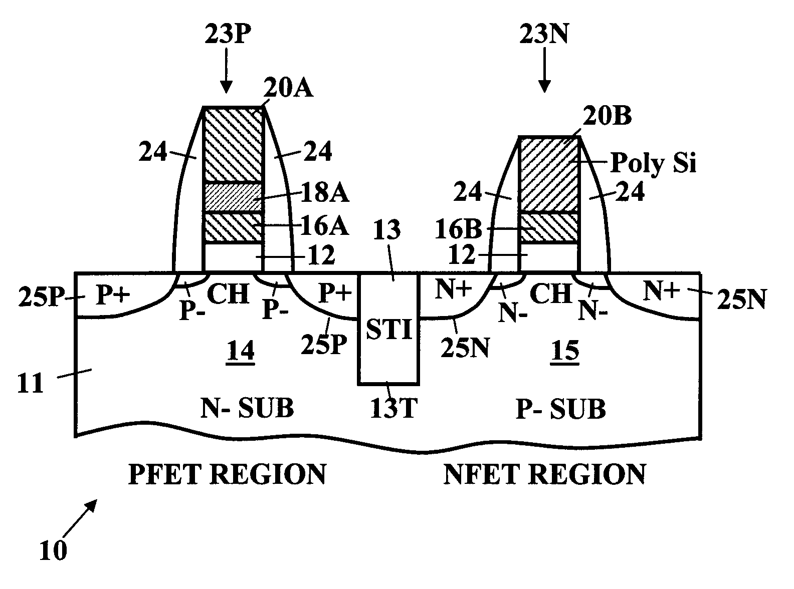
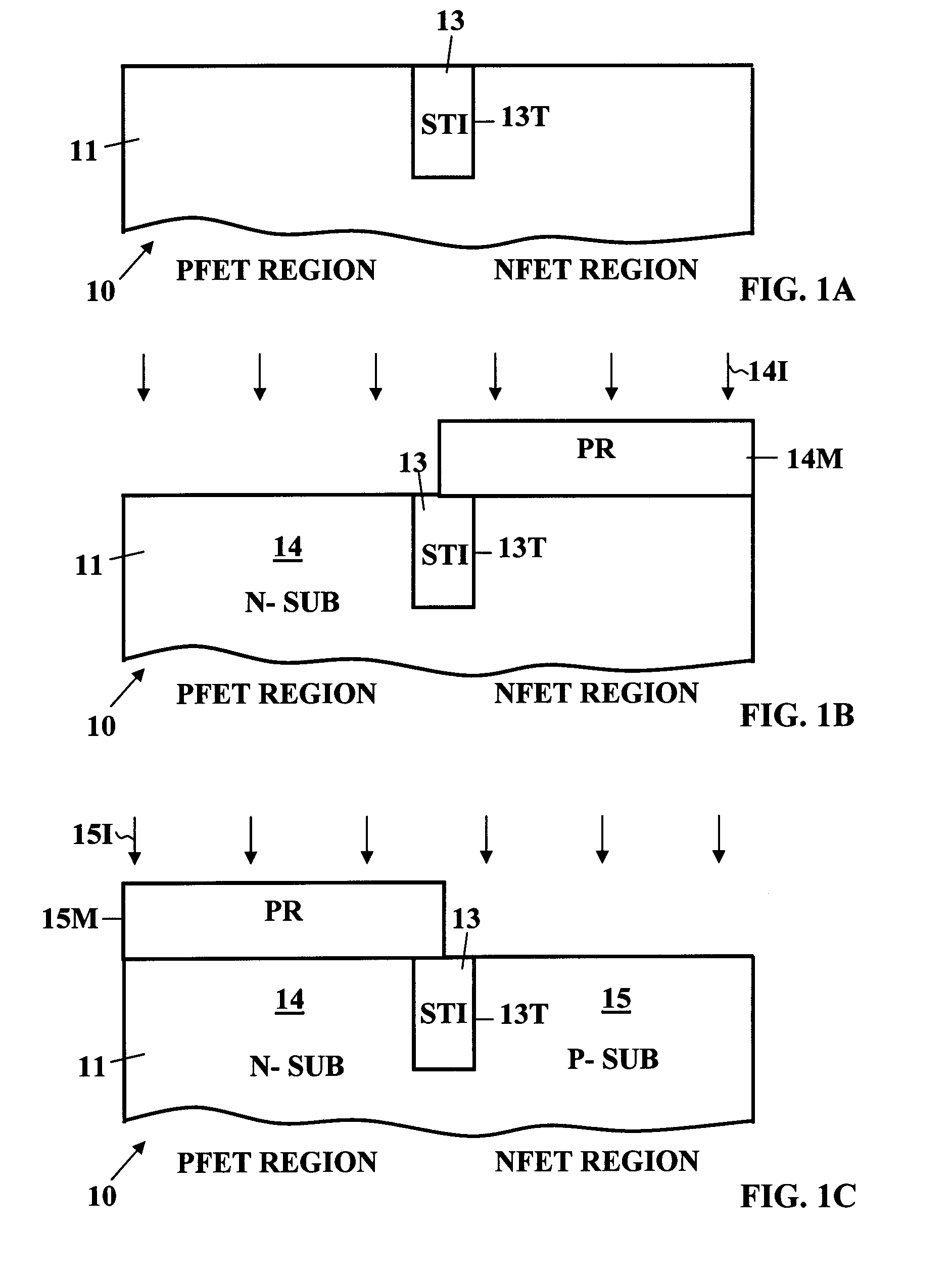
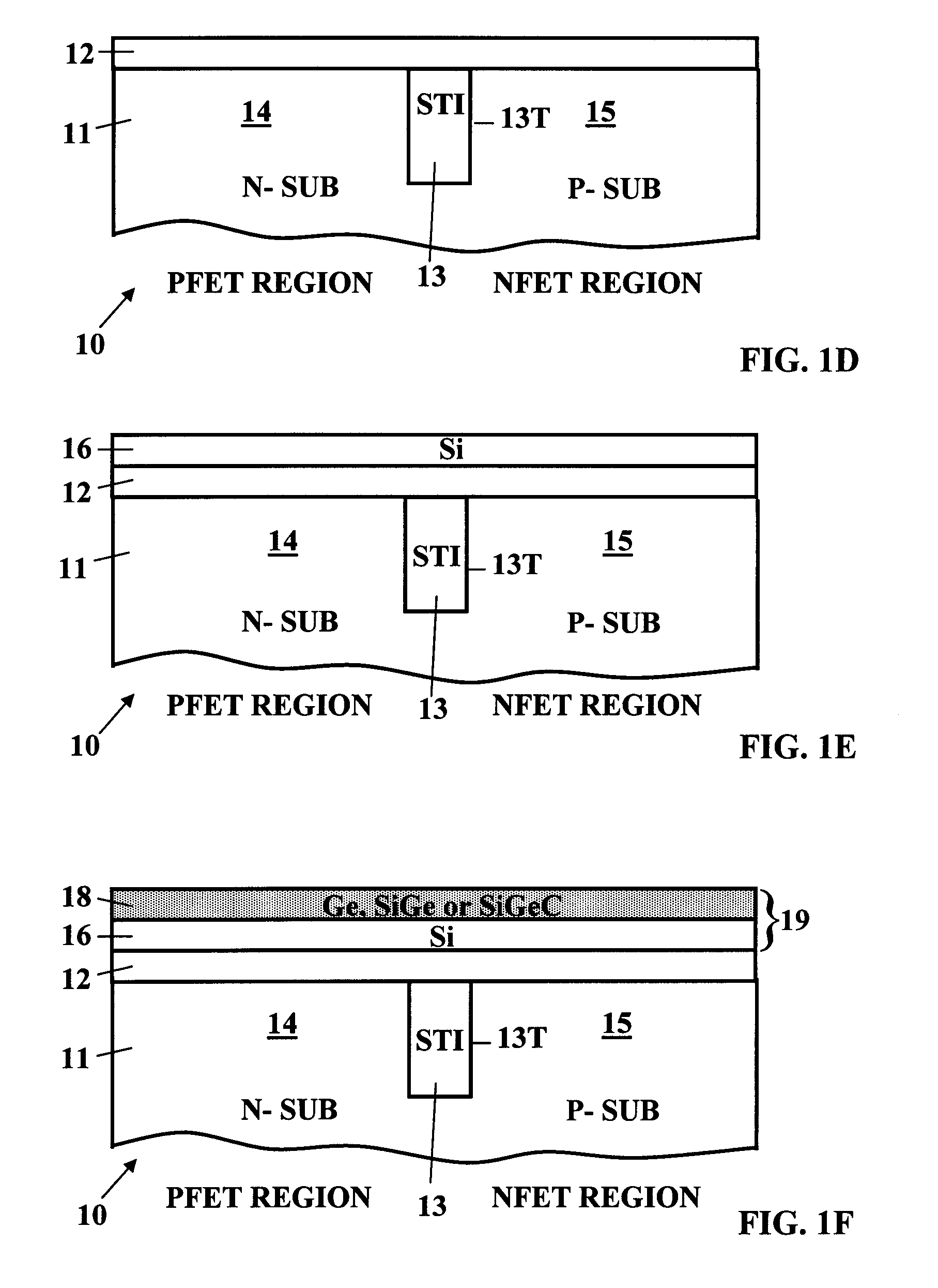
[0032]A. Deposit Shallow Trench Isolation (STI) Dielectric in Shallow Trench in Semiconductor Substrate.

[0033]FIG. 1A is a schematic sectional view of a device 10 in an early stage of manufacture comprising a semiconductor substrate 11 with a top surface in which a shallow trench 13T has been formed. The shallow trench 13T is filled with a Shallow Trench Isolation (STI) dielectric 13 formed in accordance with step 31 in FIGS. 2–4. The STI dielectric 13 separates the PFET regions on the left side of the semiconductor substrate 11 from the NFET regions on right side of semiconductor substrate 11, as will be well understood by those skilled in the art.

[0034]The substrate 11 can comprise bulk Silicon (Si), Silicon on Insulator (SOI), bulk Germanium (Ge), Si / SiGe bilayers, or Si / SiGe on insulator. Also the device structure 10 could be modified to be in the form of 3D FETs such as FinFET devices, as will be well understood by those skilled in the art of FinFET devices.

[0035]As specified i...


PUM


Abstract

Form a dielectric layer on a semiconductor substrate. Deposit an amorphous Si film or a poly-Si film on the dielectric layer. Then deposit a SiGe amorphous-Ge or polysilicon-Ge thin film theteover. Pattern and etch the SiGe film using a selective etch leaving the SiGe thin film intact in a PFET region and removing the SiGe film exposing the top surface of the Si film in an NFET region. Anneal to drive Ge into the Si film in the PFET region. Deposit a gate electrode layer covering the SiGe film in the PFET region and cover the exposed portion of the Si film in the NFET region. Pattern and etch the gate electrode layer to form gates. Form FET devices with sidewall spacers and source regions and drains regions in the substrate aligned with the gates.

Description

BACKGROUND OF THE INVENTION[0001]This invention relates to a method of manufacture of MIS (Metal Insulator Semiconductor) and MOS (Metal Oxide Semiconductor) FET (Field Effect Transistor) devices, and more particularly to a method of manufacture of Complementary MIS FET (CMIS) and Complementary MOS FET (CMOS) devices with SiGe gates.[0002]CMIS and CMOS devices include NFET and PFET devices in doped regions in a substrate and counterdoped regions in the substrate respectively. Frequently the region in the substrate in which the PFET devices are formed comprises a counterdoped well in the substrate.[0003]The metal part of a MISFET / MOSFET device is a conductor known as a gate electrode, hereinafter often referred to as gate. The gate electrode is composed of a material such as doped polysilicon or a metal conductor formed above the insulator of the MISFET generally referred to as the gate dielectric layer in a MISFET or gate oxide layer in a MOSFET. The gate electrode is part of a gate...

Claims


Application Information

Patent Timeline
IPC IPC(8): H01L21/8238H01L21/336H01L21/8242
CPCH01L21/823842H01L29/785
Inventor GREENE, BRIAN JOSEPHRIM, KERNWANN, CLEMENT
Owner GLOBALFOUNDRIES US INC
Why Eureka
Try Eureka