Semiconductor laser device and method for fabricating the same

a laser device and semiconductor technology, applied in semiconductor lasers, optical beam sources, instruments, etc., can solve the problems of low yield, significant yield drop, monolithic integration,

Inactive Publication Date: 2006-11-07
PANASONIC CORP
View PDF14 Cites 37 Cited by
  • Summary
  • Abstract
  • Description
  • Claims
  • Application Information

AI Technical Summary

Benefits of technology

[0046]Then, the semiconductor laser elements with mutually different emission wavelengths can be selectively disposed into the recessed...

Problems solved by technology

Nevertheless, in the conventional monolithic two-wavelength laser diode array, the respective active layers of the laser diodes have different compositions and thus have to be grown in different process steps, which results in the problem of low yields.
In particular, when high-output laser diodes are monolithically integrated, yields decrease significantly.
Moreover, it is very difficult, in the viewpoint of crystal growth, to monolithically integrate a gallium nitride (GaN)-based blue laser diode, which...

Method used


Image

  • Semiconductor laser device and method for fabricating the same
  • Semiconductor laser device and method for fabricating the same
  • Semiconductor laser device and method for fabricating the same

Examples


first modified example

(First Modified Example)

[0071]Hereinafter, a first modified example of the embodiment of the present invention will be described with reference to the accompanying drawings.

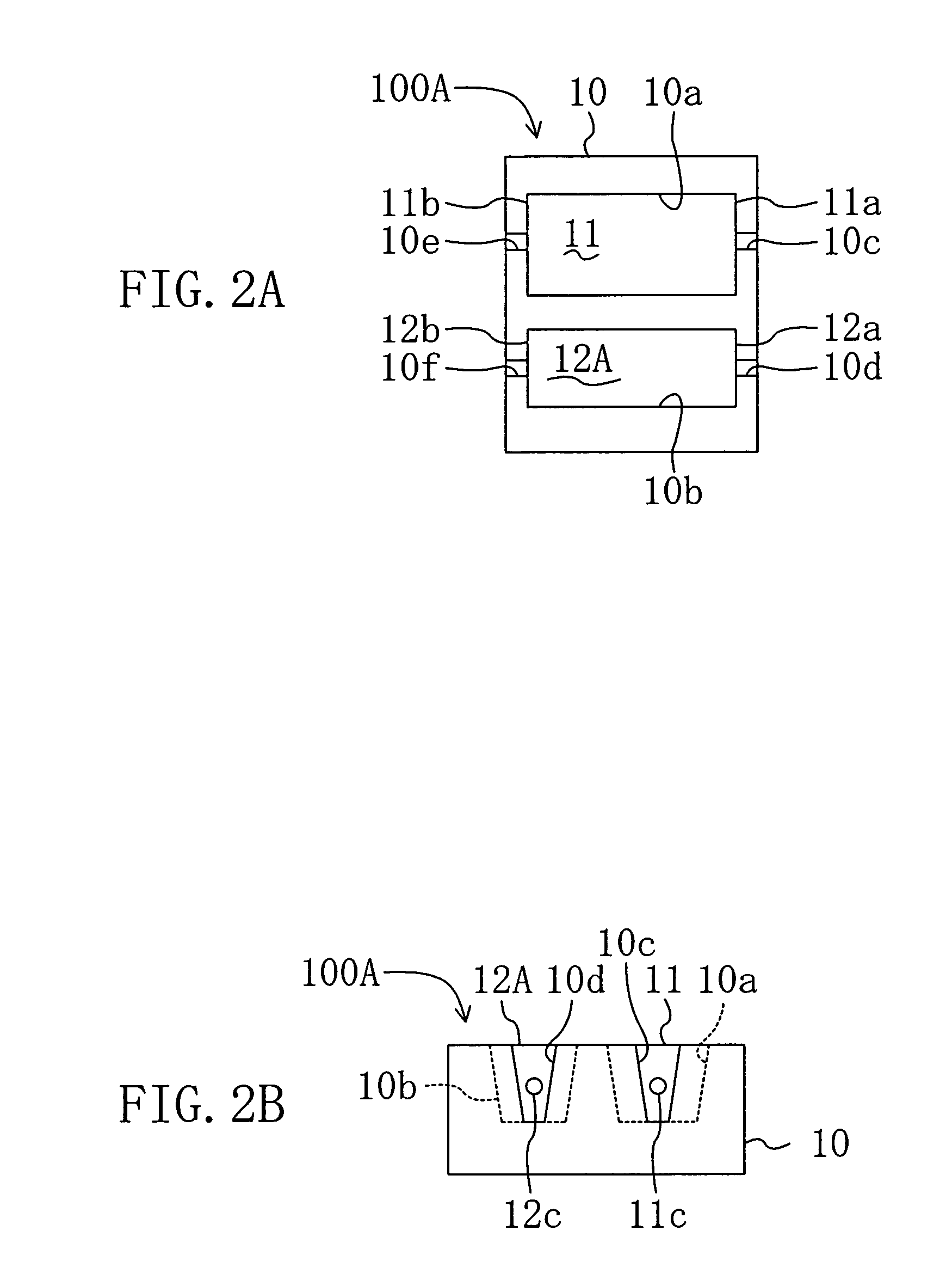
[0072]FIGS. 2A and 2B illustrate a semiconductor laser device in accordance with a first modified example of the embodiment of the present invention. FIG. 2A shows a plan configuration, and FIG. 2B shows a right-side configuration. In FIGS. 2A and 2B, the same members as those shown in FIGS. 1A and 1B are identified by the same reference numerals and the descriptions thereof will be omitted herein.

[0073]As shown in FIGS. 2A and 2B, in a semiconductor laser device 100A according to the first modified example, the width dimension of a second semiconductor laser chip 12A, which is the dimension in a vertical direction with respect to its emission direction, is made smaller than the width dimension of a first semiconductor laser chip 11. This facilitates the process of selectively disposing the semiconductor laser ch...

second modified example

[0074]Next, a second modified example of the embodiment of the present invention will be described with reference to the accompanying drawings.

[0075]FIG. 3 illustrates the plan configuration of a semiconductor laser device in accordance with a second modified example of the embodiment of the present invention. In FIG. 3, the same members as those shown in FIG. 1A are identified by the same reference numerals.

[0076]As shown in FIG. 3, in a semiconductor laser device 100B according to the second modified example, the length dimension of a second semiconductor laser chip 12B, which is the dimension in a parallel direction with respect to its emission direction, is made smaller than the length dimension of a first semiconductor laser chip 11. This also facilitates the process of disposing in the desired locations the semiconductor laser chips 11 and 12B that have mutually different laser-emitting wavelengths or mutually different optical output values. Also in this case, the laser-emitt...

third modified example

[0077]Next, a third modified example of the embodiment of the present invention will be described with reference to the accompanying drawings.

[0078]FIG. 4 illustrates the plan configuration of a semiconductor laser device in accordance with a third modified example of the embodiment of the present invention. In FIG. 4, the same members as those shown in FIG. 1A are identified by the same reference numerals.

[0079]In a semiconductor laser device 100C according to the third modified example, first and second semiconductor laser chips 11C and 12C are both high-output laser chips, and their respective end portions located on their rear facet 11b and 12b sides differ in plan configuration from their respective end portions located on their laser-emitting facet 11a and 12a sides which are situated opposite to the rear facets 11b and 12b sides. Further, as in the second modified example, the length dimension of the second semiconductor laser chip 12C is made smaller than the length dimensio...


PUM


Abstract

A semiconductor laser device includes a substrate which is made of, e.g., silicon and which has in its principal surface first and second recessed portions formed at a distance from each other. Disposed in the first recessed portion is a first semiconductor laser chip in the form of a function block, which emits an infrared laser beam. Disposed in the second recessed portion is a second semiconductor laser chip in the form of a function block, which emits a red laser beam.

Description

BACKGROUND OF THE INVENTION[0001]The present invention relates to semiconductor laser devices and methods for fabricating the devices, and more particularly relates to semiconductor laser devices which are used as a light source for the reading or writing of data from or on optical storage mediums such as compact discs and digital versatile discs, and methods for fabricating the devices.[0002]Typical digital-versatile-disc (hereinafter referred to as “DVD”) players need to function to play back compact discs (hereinafter referred to as “CDs”) in addition to DVDs, and also have to function to replay, and store data on, recordable CDs (CD-Rs) which have become widespread rapidly in recent years.[0003]As a light for replaying DVDs, a red laser beam with a wavelength in the 650 nm band is employed, while an infrared laser beam with a wavelength in the 780 nm band is used as a light for playing back CDs and CD-R discs. In the currently available DVD players, therefore, two semiconductor ...

Claims


Application Information

Patent Timeline
IPC IPC(8): H01S5/00G11B7/00G11B7/125G11B7/1275G11B7/22H01S3/04H01S5/02H01S5/0233H01S5/40
CPCG11B7/1275H01L24/95H01S5/02252H01S5/4031G11B7/22G11B2007/0006H01L2224/95085H01L2924/01004H01L2924/01013H01L2924/01015H01L2924/01033H01L2924/01049H01L2924/10329H01L2924/10349H01L2924/14H01S5/02236H01L2924/01005H01L2924/01006H01L2924/12042H01S5/023H01S5/0233H01S5/0235H01S5/02326H01L2924/00
Inventor ONOZAWA, KAZUTOSHIUEDA, TETSUZOUEDA, DAISUKE
Owner PANASONIC CORP
Why Eureka
Try Eureka