Switched capacitor integrator system

a technology of integrator system and switch capacitor, which is applied in the field of switch capacitor integrator system, can solve the problems of reducing the integration of signals, putting even more of a burden on the amplifier, and reducing the performance of the amplifier, so as to reduce the offset error, reduce the gain problem, and improve the linearity and resolution of the amplifier output voltage

Active Publication Date: 2006-11-21
ANALOG DEVICES INC
View PDF7 Cites 8 Cited by
  • Summary
  • Abstract
  • Description
  • Claims
  • Application Information

AI Technical Summary

Benefits of technology

[0007]It is a further object of this invention to provide an improved switched capacitor integrator system which reduces finite gain problems, offset errors, and significant fluctuations at the output of the amplifier.
[0008]It is a further object of this invention to provide an improved switched capacitor integrator system which eliminates capacitor divider effects particularly from the Miller capacitance from the input to the output of the input transistors, whereby the effective capacitance is (multiplied) by the gain of the transistor.
[0012]The invention results from the realization that an improved switched capacitor integrator system with reduced gain problems, reduced offset errors, and higher linearity and resolution amplifier output voltage can be effected by applying an input cascoded amplifier architecture to reduce Miller capacitance for correlated double sampling to form an integrator, even in light of multiple inputs and functions. In addition, this particular implementation of CDS, its interconnections with coexisting circuit elements, works more effectively to make the new summing junction more stable and hence improve the linearity and resolution of the amplifier outputs.
[0013]This invention features a switched capacitor integrator system including an input cascoded amplifier circuit and maintaining the stability of the summing junction and correcting for offsets which drift. There is an integrating switched capacitor circuit connected to the output of the input cascoded amplifier and to the summing junction. The integrating switched capacitor circuit includes an input switched capacitor circuit responsive to an input and connected to the summing junction. A correlated double sampling capacitor circuit includes an offset capacitor interconnected between the summing junction and the input of the input cascoded amplifier circuit.
[0014]In the preferred embodiment the input switched capacitor circuit may include a variable capacitance circuit. The variable capacitance circuit may include a plurality of capacitors. It may include a plurality of switches at its input. It may include a plurality of switches at its output. The correlated double sampling capacitor circuit may include a hold capacitor interconnected to the output of the cascoded amplifier circuit and through a first switch to the input of the cascoded amplifier circuit and through a second switch to a bias voltage. The hold capacitor may be connected to the output of the cascoded amplifier circuit through a third switch. The input switched capacitor circuit may include a gain switching circuit. The summing junction may be adapted for receiving additional inputs. The additional inputs may include a digital to analog converter circuit. The inputs may include continuous voltage inputs. It may include a centering circuit and the additional inputs may include a centering circuit output. The centering circuit may include a center switching circuit responsive to an input source. The centering circuit may include a plurality of capacitors in the switching circuit to select a capacitor to provide a predetermined centering voltage. The system may be a single ended system. It may be a differential system and there may be a second complementary switched capacitor circuit and a second complementary correlated double sampling circuit. The input cascoded amplifier circuit may include a plurality of stages and at least the first stage input may be cascoded. The input stage of the amplifier may include an input differential cascoded transistor pair for reducing Miller effects from the input to the output of the input differential transistor pair. The cascoded amplifier circuit may include load circuits which may be e.g., current sources, resistors or diode connected MOSFET's.

Problems solved by technology

The performance is limited (1) by amplifier problems with offsets which drift with temperature, (2) by limited amplifier gain, (3) by input signal offsets and range problems, (4) by containing too many or too large components, (5) by containing components which do not track the temperature or supply characteristics of the other components, and (6) by extra components which introduce residual errors such as switch charge injection.
This puts even more of a burden on the amplifier and degrades the integration of the signals.
The previous solutions either address incorrectly or do not address the architecture of the amplifier which is critical for CDS (including predictive CDS, PCDS) implementation, because it would otherwise degrade the apparent gain of the amplifier through undesired charge sharing on capacitor dividers due to undesirable Miller capacitive effects occurring from the input to the output of the input transistors.
Also the prior art does not utilize the additional advantages afforded by CDS through strategic placement of the switches and capacitors, nor do they reduce the number of components nor size of the implementations as much as possible, nor allow better temperature tracking of the components.

Method used


Image

  • Switched capacitor integrator system
  • Switched capacitor integrator system
  • Switched capacitor integrator system

Examples


Embodiment Construction

[0025]Aside from the preferred embodiment or embodiments disclosed below, this invention is capable of other embodiments and of being practiced or being carried out in various ways. Thus, it is to be understood that the invention is not limited in its application to the details of construction and the arrangements of components set forth in the following description or illustrated in the drawings.

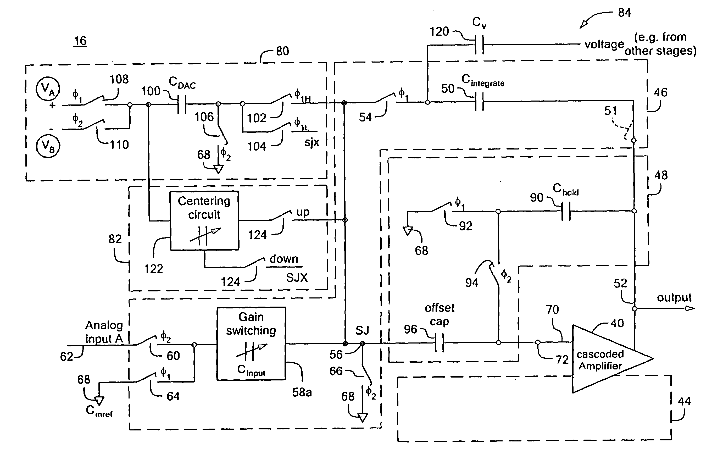
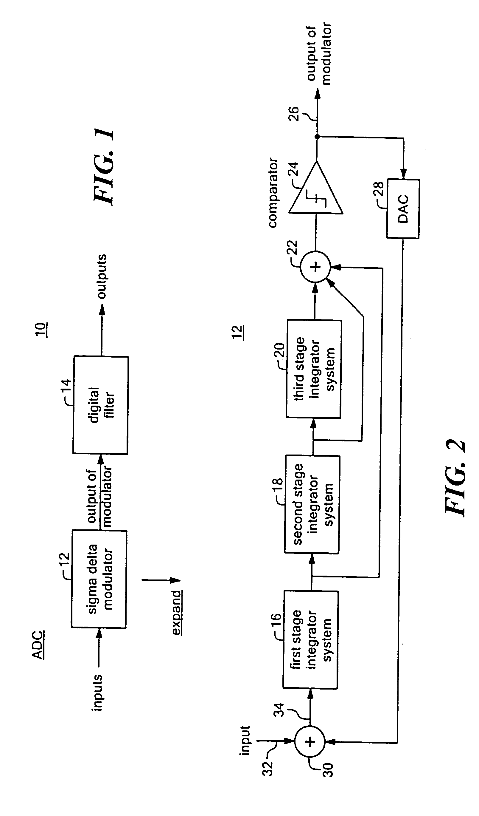
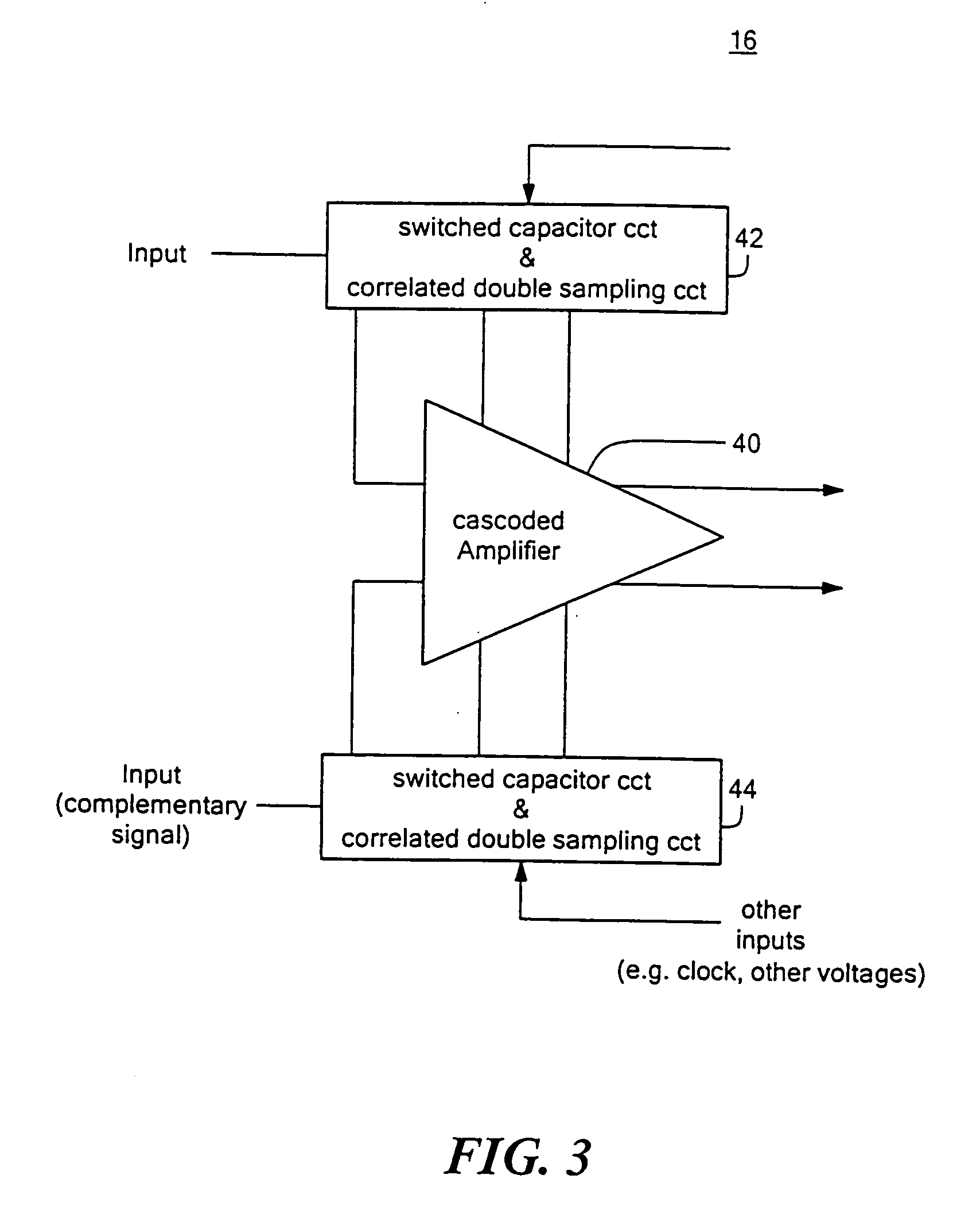
[0026]There is shown in FIG. 1 a sigma-delta type of analog to digital converter 10 including a sigma delta modulator 12 and digital filter 14. The sigma-delta modulator 12 is a typical circuit that is implemented with one or more integrator system stages, FIG. 2; a first stage integrator system 16, second stage integrator system 18, and third stage integrator 20. The outputs of each of the integrator systems are combined in summing circuit 22 and submitted to comparator 24 whose output 26 constitutes the output of the sigma delta modulator 12. There is a feedback circuit through digital to...


PUM


Abstract

A switched capacitor integrator system includes an input cascoded amplifier circuit; a summing junction; an integrating switched capacitor circuit connected to the output of the input cascoded amplifier circuit and to the summing junction; the integrating switched capacitor circuit including an input switched capacitor circuit responsive to an input and connected to the summing junction; and a correlated double sampling capacitor circuit including an offset capacitor interconnected between the summing junction and the input of the input cascoded amplifier circuit.

Description

FIELD OF THE INVENTION[0001]This invention relates to a switched capacitor integrator system.BACKGROUND OF THE INVENTION[0002]High performance system integrated circuits (IC) such as for wireless telecommunications or for internet data communications often need critical circuits including sigma delta analog to digital converters (ADC), filters, integrators, sample-holds, gain stages, delay stages, and so on, all of which contain a switched capacitor integrator circuit. These circuits require high resolution, good linearity and DC offset rejection for applications like temperature monitoring, data acquisition, and voice digitization. The key component of the integrator is its amplifier and the constancy of the summing junction. The performance is limited (1) by amplifier problems with offsets which drift with temperature, (2) by limited amplifier gain, (3) by input signal offsets and range problems, (4) by containing too many or too large components, (5) by containing components whic...

Claims


Application Information

Patent Timeline
Patent Type & Authority Patents(United States)
IPC IPC(8): G06F7/64G05F1/40G05F1/56G06G7/184H03M1/50H03M1/66H03M3/00
CPCG06G7/184H03M3/43H03M3/452
Inventor WU, DOLLYFERGUSON, JR., PAUL
Owner ANALOG DEVICES INC
Why Eureka
Try Eureka