Circuit board

a technology of circuit board and semiconductor, applied in the direction of semiconductor/solid-state device details, printed circuit details, solid-state devices, etc., can solve the problems of large problems, increased stress under the terminal, and cracks in ceramics, so as to prolong the life time of thermal fatigue, reduce the deformation of the fixing bolt, and reduce the strain of the solder

Inactive Publication Date: 2006-11-28
FITEL USA CORP
View PDF14 Cites 13 Cited by
  • Summary
  • Abstract
  • Description
  • Claims
  • Application Information

AI Technical Summary

Benefits of technology

[0024]The first problem is that a crack occurs in the ceramic at a position under a Cu thin plate on the ceramic substrate where an electrode terminal is bonded by solder. Since the linear expansion coefficients of the ceramic substrate and the Mo plate are close to each other, the thermal stress acting on the solder between the ceramic substrate and the Mo plate is decreased. That is, the ceramic substrate and the Mo plate are thermally deformed as if both are formed of one material. Therefore, the thermal stress between the Cu thin plate on the ceramic substrate and the ceramic substrate is increased. It has been estimated from a result of thermal stress analysis that when a Cu terminal is attached onto the Cu thin plate, the thermal stress under the terminal is extremely increased to cause cracks in the ceramic under the Cu thin plate. Therefore, it is necessary to prevent the ceramic substrate from being damaged by suppressing the thermal deformation of the Cu thin plate and decreasing the thermal stress between the Cu thin plate and the ceramic substrate in such a structure that the Cu thin plate portion to be attached with the Cu terminal is not bonded to the ceramic substrate, that is, in a floating state, or that the portion to be attached with the Cu terminal is not placed in the periphery of the Cu thin plate pattern, but is placed in the inner side of the Cu thin plate pattern, or that a material having a small linear expansion coefficient such as Mo is inserted between the Cu terminal and the Cu thin plate.
[0051]In the circuit board, the insulating capacitance component (Cb) by the portion of the insulator plate contacting to the gap and the insulating capacitance component (Cg) by the gap are connected in series. Therefore, when voltage (Vl) is applied to the circuit board of a semiconductor device mounting the circuit board, the voltage is split into each of the insulating capacitance components. Therein, according to the present invention, since a dielectric material is filled in the gap and the insulating capacitance component of this portion is, therefore, increased, the voltage (Vg) split in the gap can be decreased (Vg=Vl×Cb / (Cg+Cb)). Accordingly, the partial discharge in the gap can be suppressed.

Problems solved by technology

However, the inventors have found that simply using Mo instead of Cu, which is conventionally used, leads to three large problems.
The first problem is that a crack occurs in the ceramic at a position under a Cu thin plate on the ceramic substrate where an electrode terminal is bonded by solder.
It has been estimated from a result of thermal stress analysis that when a Cu terminal is attached onto the Cu thin plate, the thermal stress under the terminal is extremely increased to cause cracks in the ceramic under the Cu thin plate.
The second problem is that loosening of a fixing bolt or damage of the fixing bolt occurs by thermal deformation due to the difference in linear expansion coefficients the metallic base of a semiconductor device and the member to fix the semiconductor device.
The third problem is that there is presently no material having a linear expansion coefficient which is close to that of silicon and a thermal conductivity which is as large as that of Cu.
When Mo is used for the metallic base, the heat transferred from the chip is not sufficiently diffused and, accordingly, the heat has to be dissipated from a small area of the metallic base.
Although it is preferable that the surface of the gel is coated with a mold release agent, there is no proper material in the state of the art.

Method used


Image

  • Circuit board
  • Circuit board
  • Circuit board

Examples


first embodiment

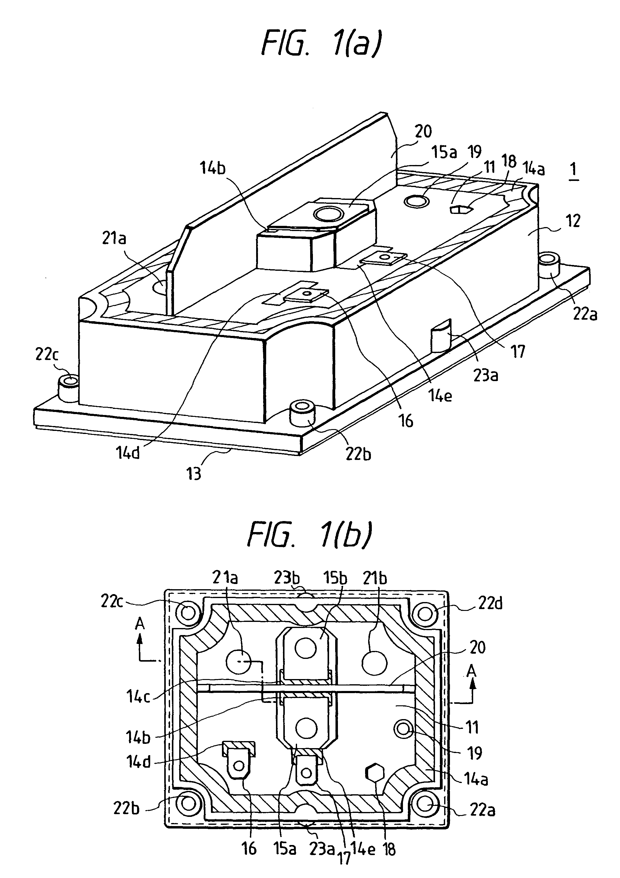
[0117]Firstly, a semiconductor module according to the present invention will be described, referring to FIG. 18 to FIG. 24. The semiconductor module of this embodiment mounts three diode elements 101, 102, 103 of same kind and same size as shown in FIG. 18. Each of the diode elements 101, 102, 103 is square-plate-shaped, and on the top surface of the diode element there is an anode electrode (input electrode) through which current flows in from the external, and on the bottom surface there is a cathode electrode (output electrode) through which current floes out to the external.

[0118]The semiconductor module comprises, as shown in FIG. 18 to FIG. 20, the three diodes 101, 102, 103 as described above, a metallic supporting board 114, a rectangular insulator substrate 106 provided on the supporting board 114, an anode side conductor pattern 105 electrically connected to the anode electrodes on the top surfaces of the diode elements 101, 102, 103 in parallel, a cathode side conductor ...

second embodiment

[0135]a semiconductor module according to the present invention will be described below, referring to FIG. 25 and FIG. 26.

[0136]The semiconductor module in this embodiment comprises two sets of insulator substrates each of which mounts three IGBT elements and one diode element as shown in FIG. 25. The IGBT element is square plate-shaped, having an emitter electrode (input electrode) and a gate electrode (control electrode) on the top surface, and a collector electrode (output electrode) on the bottom surface.

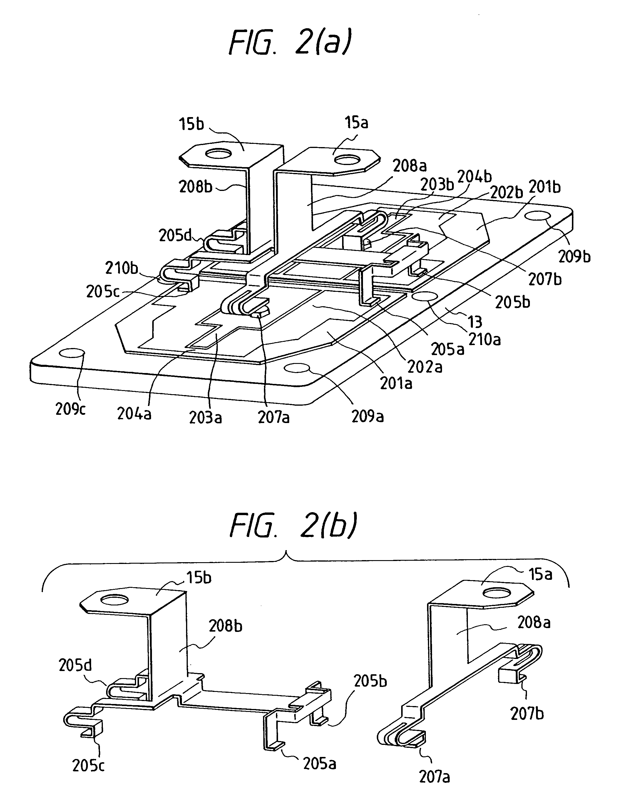
[0137]On a metallic supporting board 114, two insulator substrates 106, 106 made of aluminum nitride are arranged symmetrically in regard to the center line 622 of the metallic supporting board 114. On one of the insulator substrate 106, conductor patterns 610, 611, 614 made of copper are formed. Among the conductor patterns 610, 611, 614, on the collector side conductor pattern 610, the IGBT elements 601, 602, 603 and the diode element 607 are arranged and a collector side conn...

fourth embodiment

[0150]a semiconductor module is an IGBT module mounting two IGBT elements 601, 603 and one diode element 607 as shown in FIG. 29. On a metallic supporting board 114, an insulator substrate 106 is arranged by putting its center on the center line 622. On the insulator substrate 106, a collector side conductor pattern 610, an emitter side conductor pattern 614 and a gate side conductor pattern 611 are formed so that the positions and the shapes are symmetrical in regard to the center line 622. On the collector side conductor pattern 610, the IGBT elements 601, 603 and the diode element 607 are arranged and a collector side connecting terminal 612 is bonded. On the gate side conductor pattern 611, two gate resistor elements 609, 609 are arranged and a gate side terminal 620 is bonded. On the emitter side conductor pattern 614, an emitter side connecting terminal 616 and an emitter auxiliary connecting terminal 618 are bonded. The emitter auxiliary connecting terminal 618 has a leg comm...


PUM


Abstract

A semiconductor device in which electrodes of a plurality of semiconductor elements are bonded onto at least one of a plurality of electrode patterns on an insulator substrate, the other surface of the insulator substrate being bonded to a heat dissipating base. The upper surface of the heat dissipating base is covered with a member for cutting off the semiconductor elements from the outer environment. Terminals electrically connect the electrodes on said insulator substrate and the electrode placed outside the cutoff member. The material of the heat dissipating base has a linear expanding coefficient larger than that of the semiconductor element and smaller than three times that of the semiconductor element, and a thermal conductivity larger than 100 W / mK. The semiconductor elements are arranged on at least one electrode surface and in at least two regions divided by the other electrode surface on the insulator substrate.

Description

CROSS-REFERENCE TO RELATED APPLICATIONS[0001]This is a Continuation application of application Ser. No. 10 / 101,463, filed Mar. 20, 2002 (now Abandoned); which is a Continuation of application Ser. No. 09 / 385,632, filed Aug. 27, 1998 (now U.S. Pat. No. 6,434,008); which is a divisional of application Ser. No. 08 / 539,075, filed on Oct. 4, 1995 (now U.S. Pat. No. 5,956,231) (which was a CPA application of the originally filed application) the entire disclosures of which are hereby incorporated by reference.BACKGROUND OF THE INVENTION [0002]1. Field of the Invention[0003]The present invention relates to a semiconductor module and a semiconductor device using a power semiconductor element, and more particularly relates to a semiconductor device which is useful, for example, for inverters and converters.[0004]2. Description of the Related Art[0005]In various kinds of motor control, GTOs (Gate Turn Off Thyristors) have been used for large power applications and transistors have been used f...

Claims


Application Information

Patent Timeline
Patent Type & Authority Patents(United States)
IPC IPC(8): H05K1/03H01L23/049H01L23/495H01L25/065H02M7/00
CPCH01L23/049H01L24/49H01L25/0655H01L25/072H01L25/18H02M7/003H01L23/49562H01L2924/1305H01L2224/45015H01L2224/48011H01L2224/48091H01L2224/48472H01L2224/49111H01L2224/49171H01L2224/4943H01L2224/73265H01L2924/01003H01L2924/01005H01L2924/01006H01L2924/01013H01L2924/01014H01L2924/01022H01L2924/01025H01L2924/01028H01L2924/01029H01L2924/01033H01L2924/01039H01L2924/01042H01L2924/01047H01L2924/0105H01L2924/01061H01L2924/01074H01L2924/01078H01L2924/01079H01L2924/01082H01L2924/01322H01L2924/13055H01L2924/19043H01L2924/2076H01L2924/30105H01L2924/30107H01L2924/3025H01L24/45H01L24/48H01L2924/01019H01L2924/01041H01L2924/014H01L2224/32225H01L2224/48227H01L2924/13091H01L2924/1301H01L2924/00014H01L2924/00H01L2924/00012H01L2224/451H01L2924/351H01L2924/15787H01L2924/181H01L2224/49431H01L2224/49113H01L2224/05599H01L29/70
Inventor YAMADA, KAZUJITANAKA, AKIRASAITO, RYUICHIKURIHARA, YASUTOSHIKUSHIMA, TADAOHARAMAKI, TAKASHIKOIKE, YOSHIHIKOHOSOKAWA, TAKASHISAWAHATA, MAMORUKOIZUMI, MASAHIROONUKI, JINSUZUKI, KAZUHIROKOBAYASHI, ISAOSHIMIZU, HIDEOHIGASHIMURA, YUTAKASEKINE, SHIGEKIKOIKE, NOBUYAKOKUBUN, HIDEYA
Owner FITEL USA CORP
Why Eureka
Try Eureka