

Holding device, in particular for fixing a semiconductor wafer in a plasma etching device, and method for supplying heat to or dissipating heat from a substrate
a plasma etching and semiconductor technology, which is applied in the direction of electrostatic charges, electrical devices, capacitors, etc., can solve the problems of significant increase in the etching rate in the edge area of the wafer, detrimental effects in the vicinity of the substrate electrode, and significant non-homogeneity of etching, so as to improve the stability and uniformity of etching, improve the effect of electrostatic clamping force and simplify the fixation and release of the wafer
- Summary
- Abstract
- Description
- Claims
- Application Information
AI Technical Summary
Benefits of technology
Problems solved by technology
Method used
Image

Examples
Embodiment Construction
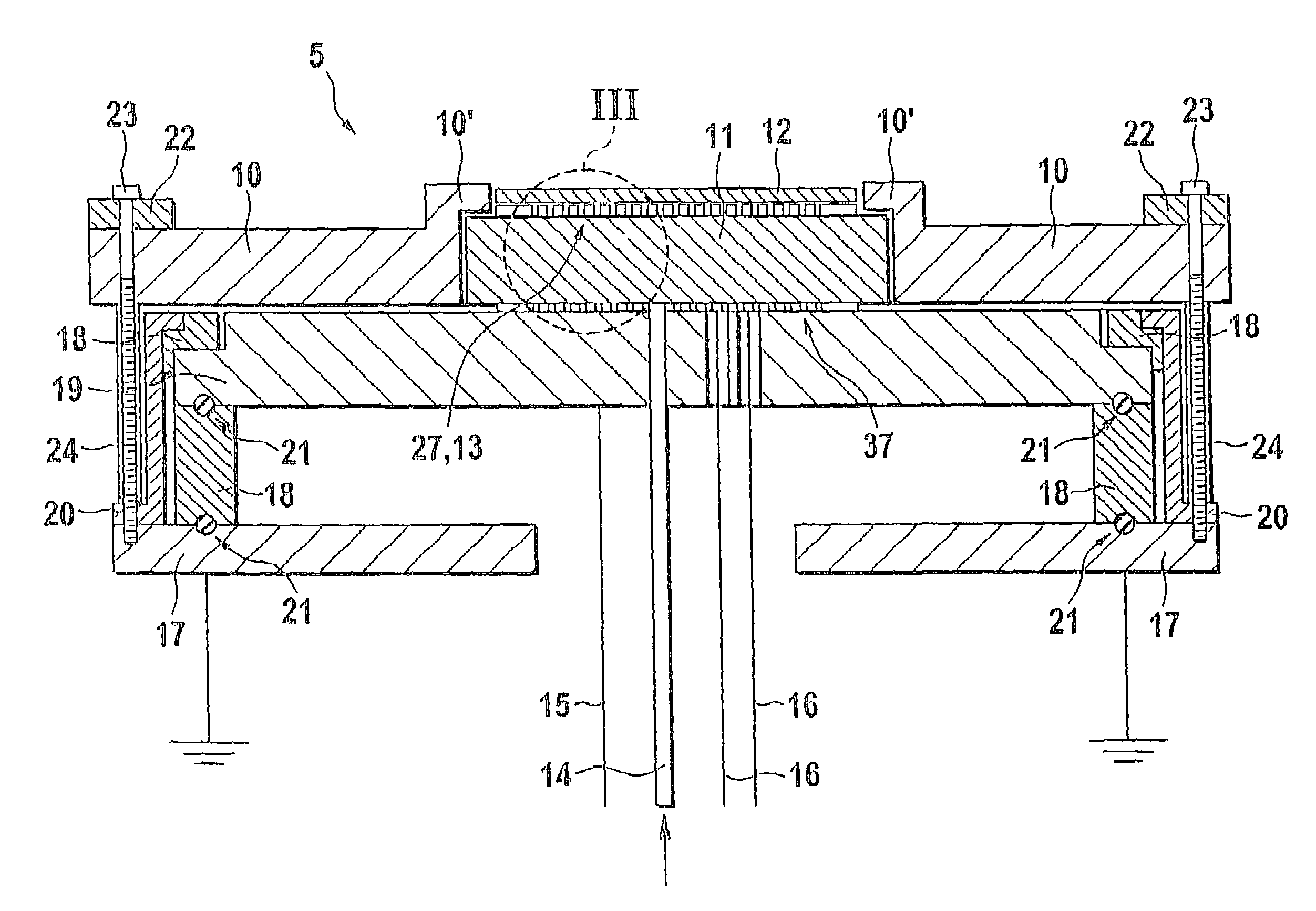
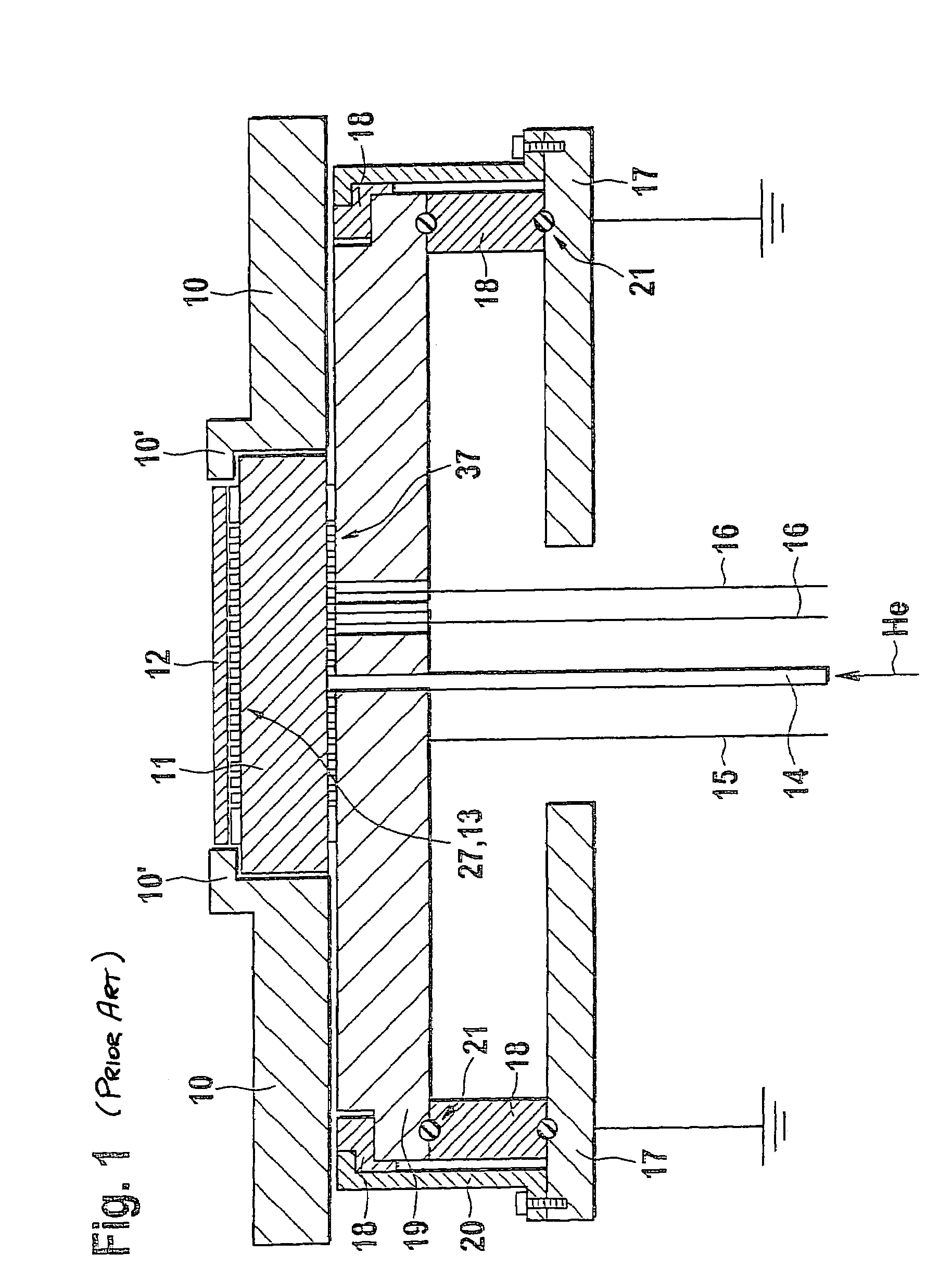
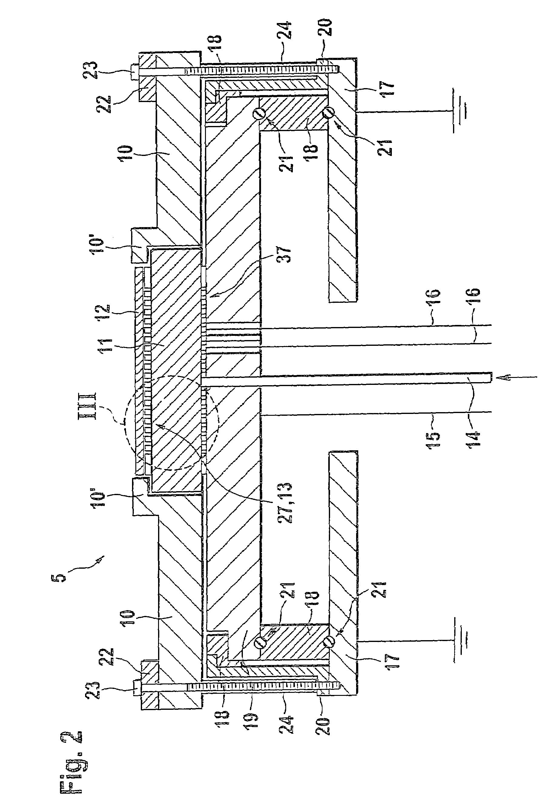
[0018]FIG. 1 initially illustrates an electrostatic “chuck” from the related art, i.e., an electrostatic holding device for a substrate 12, for example a conventional silicon wafer. Under substrate 12 is a holding element 11 that secures this, for example an electrostatic “chuck” designed in the form of a holding plate. Holding element 11 is also placed on a metallic substrate electrode 19, which is connected via insulators 18, which may be ceramic insulators 18, with a base or support 17, which is also made of a metal. To ensure the vacuum seal, seals 21, for example O-rings of rubber, are provided between insulators 18 and substrate electrode 19 or between insulators 18 and base 17.
[0019]FIG. 1 also shows that base 17 is connected to substrate electrode 19 via a metallic holder 20, ceramic insulators 18 may also be provided between holder 20 and substrate electrode 19, so that base 17 is completely electrically insulated from substrate electrode 19. Furthermore, a ceramic plate is...
PUM
 Abstract
Description
Claims
Application Information