Composite tantalum nitride/tantalum copper capping layer

a tantalum nitride and copper capping layer technology, applied in semiconductor devices, semiconductor/solid-state device details, electrical apparatus, etc., can solve the problems of escalating requirements that are difficult to meet, rc delay caused by interconnect wiring increases, reliability issues have evolved, etc., to achieve high reliability, reduce interconnect capacitance, the effect of improving the electromigration and stress migration performan

Active Publication Date: 2007-01-02
INNOVATIVE FOUNDRY TECH LLC
View PDF15 Cites 14 Cited by
  • Summary
  • Abstract
  • Description
  • Claims
  • Application Information

AI Technical Summary

Benefits of technology

[0010]An advantage of the present invention is a method of manufacturing a semiconductor device having highly reliable capped Cu or Cu alloy interconnect with reduced interconnect capacitance and improved electromigration and stress migration performance.
[0011]Another advantage of the present invention is a semiconductor device comprising a reliably capped Cu or Cu alloy interconnect member with reduced interconnect capacitance and improved electromigration and stress migration performance.
[0012]Additional advantages and other features of the present invention will be set forth in the description which follows and, in part, will become apparent to those having ordinary skill in the art upon examination of the following or may be learned from the practice of the present invention. The advantages of the present invention may be realized and obtained as particularly pointed out in the appended claims.
[0013]According to the present invention, the foregoing and other advantages are achieved in part by a method of manufacturing a semiconductor device, the method comprising: forming an opening in the first dielectric layer; filling the opening with copper (Cu) or a Cu alloy; and forming a composite capping layer on the Cu or Cu alloy, the composite capping layer comprising: a layer of tantalum nitride on an upper surface of the Cu or Cu

Problems solved by technology

Such escalating requirements have been found difficult to satisfy in terms of providing a low R×C (resistance×capacitance) interconnect pattern with electromigration resistance, particularly wherein submicron vias, contacts and trenches have high aspect ratios imposed by miniaturization.
As the length of metal interconnects increases and cross-sectional areas and distances between interconnects decrease, the R×C delay caused by the interconnect wiring increases.
The technological benefits of Cu, such as reduced R×C delay are clear; however, various reliability issues have evolved.
There are additional problems attendant upon conventional Cu interconnect methodology employing a diffusion barrier layer (capping layer).
It was found, however, that capping layers, such as silicon nitride, deposited by plasma enhanced chemical vapor deposition (PECVD

Method used


Image

  • Composite tantalum nitride/tantalum copper capping layer
  • Composite tantalum nitride/tantalum copper capping layer
  • Composite tantalum nitride/tantalum copper capping layer

Examples


Embodiment Construction

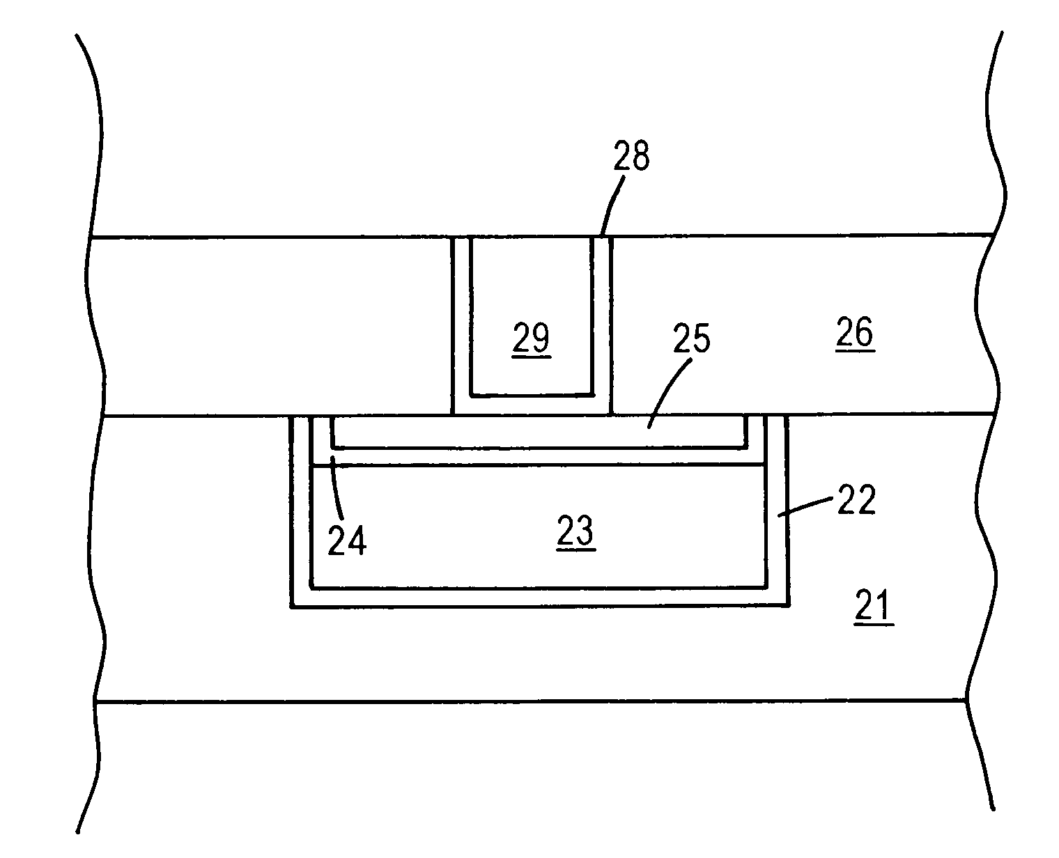
[0020]Conventional methodology for fabricating semiconductor devices with capped inlaid Cu are accompanied by via resistance, electromigration and stress migration problems. In copending application Ser. No. 10 / 791,904, filed on Mar. 4, 2004 such problems are addressed by forming a composite capping layer comprising a thin layer of beta (β)-Ta on an upper surface of the inlaid Cu, a thin layer of tantalum nitride on the layer of β-Ta and a layer of α-Ta on the thin titanium nitride layer. The resulting interconnect structure exhibits reduced via resistance, reduced voiding under the via, improved stress migration performance and improved electromigration performance. Further, by avoiding the need to remove the Ta layer, which in itself is difficult, slow and unproven, manufacturing throughput is increased, manufacturing costs decreased, beveling of via corners avoided and Cu contamination reduced.

[0021]The present invention constitutes an improvement over the invention disclosed on ...


PUM


Abstract

Electromigration and stress migration of Cu interconnects are significantly reduced by forming a composite capping layer comprising a layer of tantalum nitride on the upper surface of the inlaid Cu and a layer of α-Ta on the titanium nitride layer. Embodiments include forming a recess in an upper surface of an upper surface of Cu inlaid in a dielectric layer, depositing a layer of titanium nitride of a thickness of 20 Å to 100 Å and then depositing a layer of α-Ta at a thickness of 200 Å to 500 Å.

Description

FIELD OF THE INVENTION[0001]The present invention relates to copper (Cu) and / or Cu alloy metallization in semiconductor devices, and to a method for forming reliably capped Cu or Cu alloy interconnects. The present invention is particularly applicable to manufacturing high speed integrated circuits having submicron design features, and high conductivity interconnects with improved electromigration resistance and improved stress migration resistance.BACKGROUND ART[0002]The escalating requirements for high density and performance associated with ultra large scale integration semiconductor wiring require responsive changes in interconnection technology. Such escalating requirements have been found difficult to satisfy in terms of providing a low R×C (resistance×capacitance) interconnect pattern with electromigration resistance, particularly wherein submicron vias, contacts and trenches have high aspect ratios imposed by miniaturization. High performance microprocessor applications requ...

Claims


Application Information

Patent Timeline
IPC IPC(8): H01L23/48
CPCH01L21/2855H01L21/76843H01L21/76849H01L21/76846Y10S438/927
Inventor ERB, DARRELL M.AVANZINO, STEVEN C.WOO, CHRISTY MEI-CHU
Owner INNOVATIVE FOUNDRY TECH LLC
Why Eureka
Try Eureka