

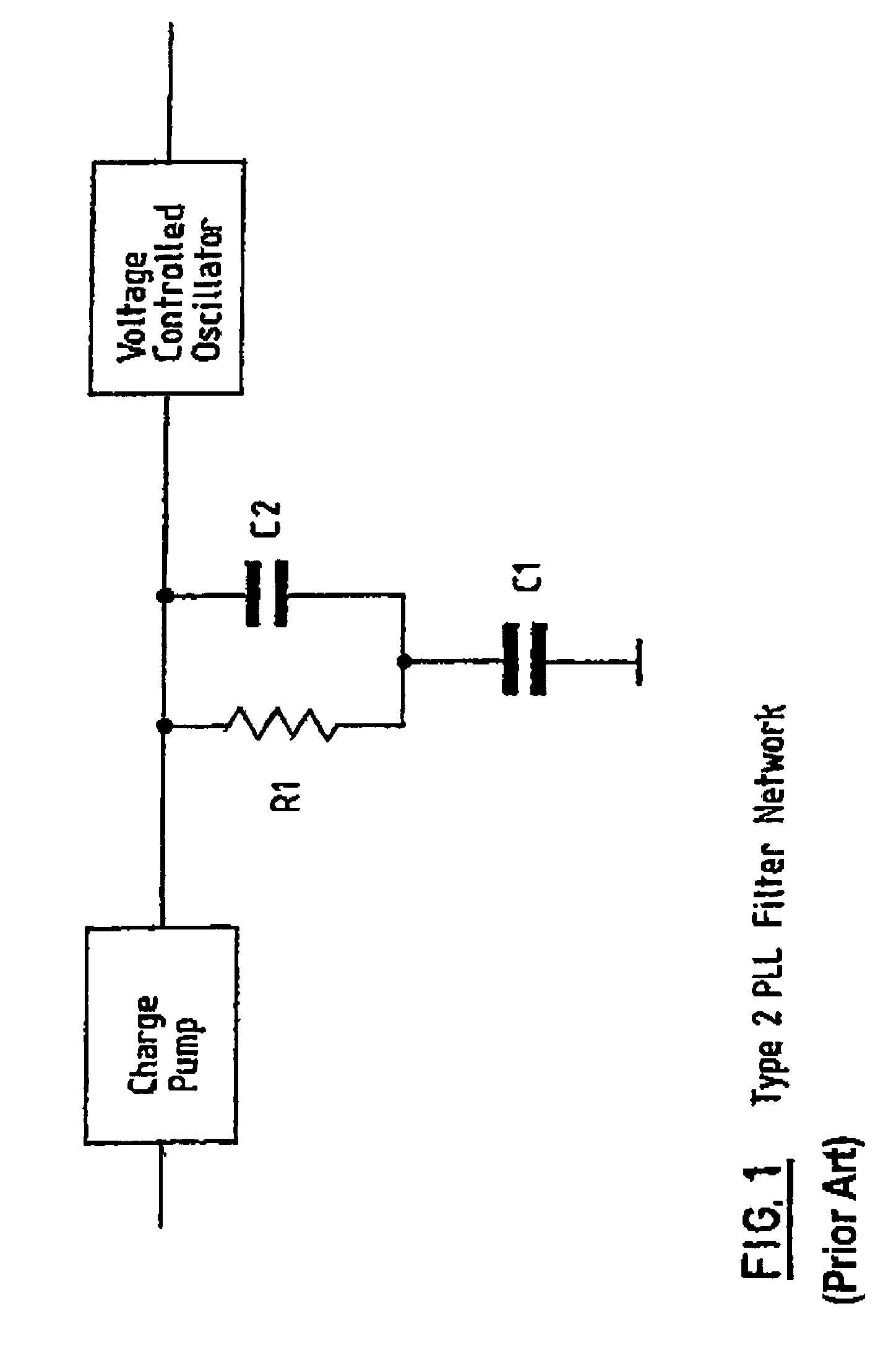
Semiconductor type two phase locked loop filter
a phase locked loop and semiconductor technology, applied in the direction of pulse automatic control, oscillator generator, pulse technique, etc., can solve the problems of difficult design of this arrangement, difficult to accurately calculate cb>1/b>, and more complexity, so as to facilitate the making of floating capacitors
- Summary
- Abstract
- Description
- Claims
- Application Information
AI Technical Summary
Benefits of technology
Problems solved by technology
Method used
Image

Examples
Embodiment Construction
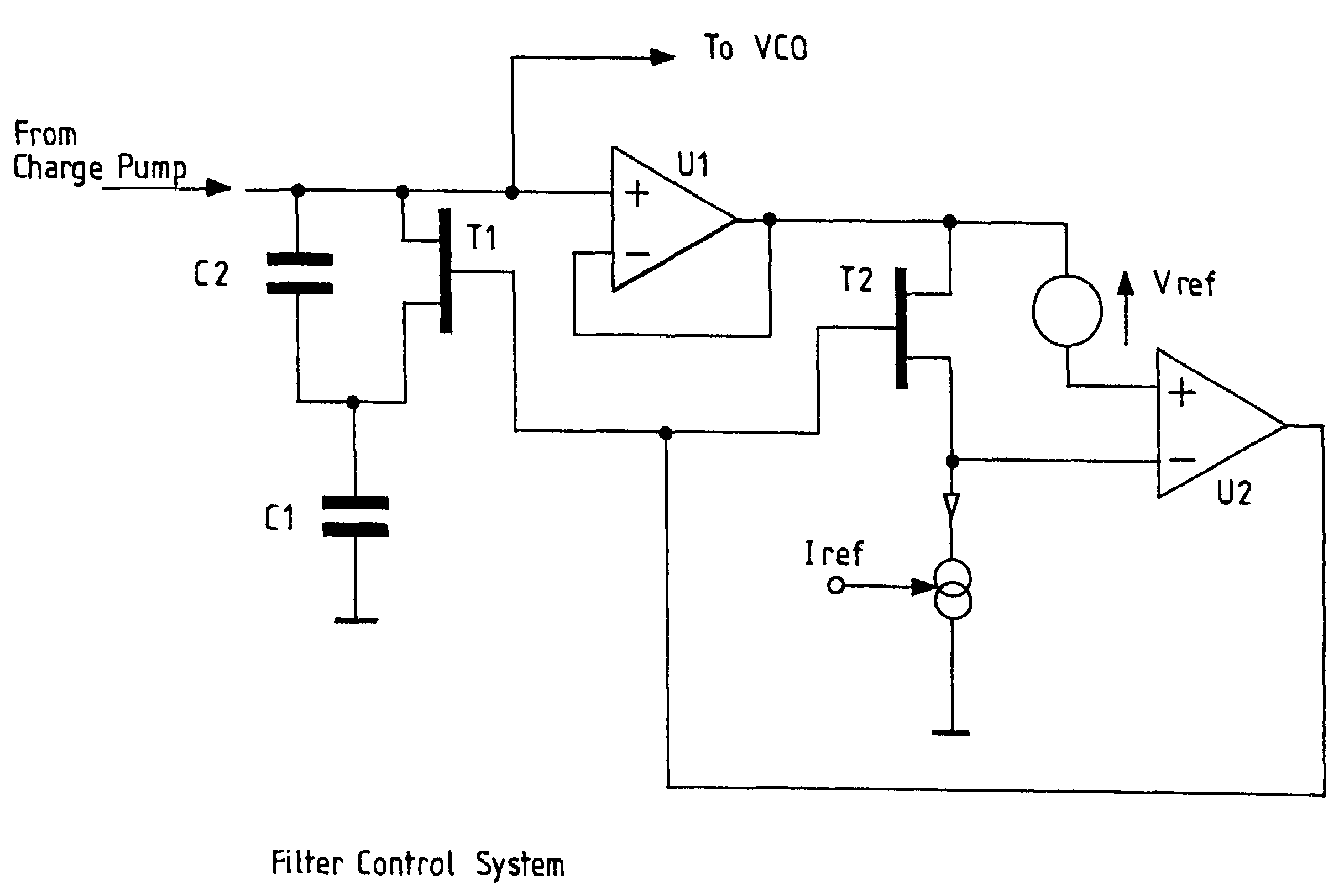
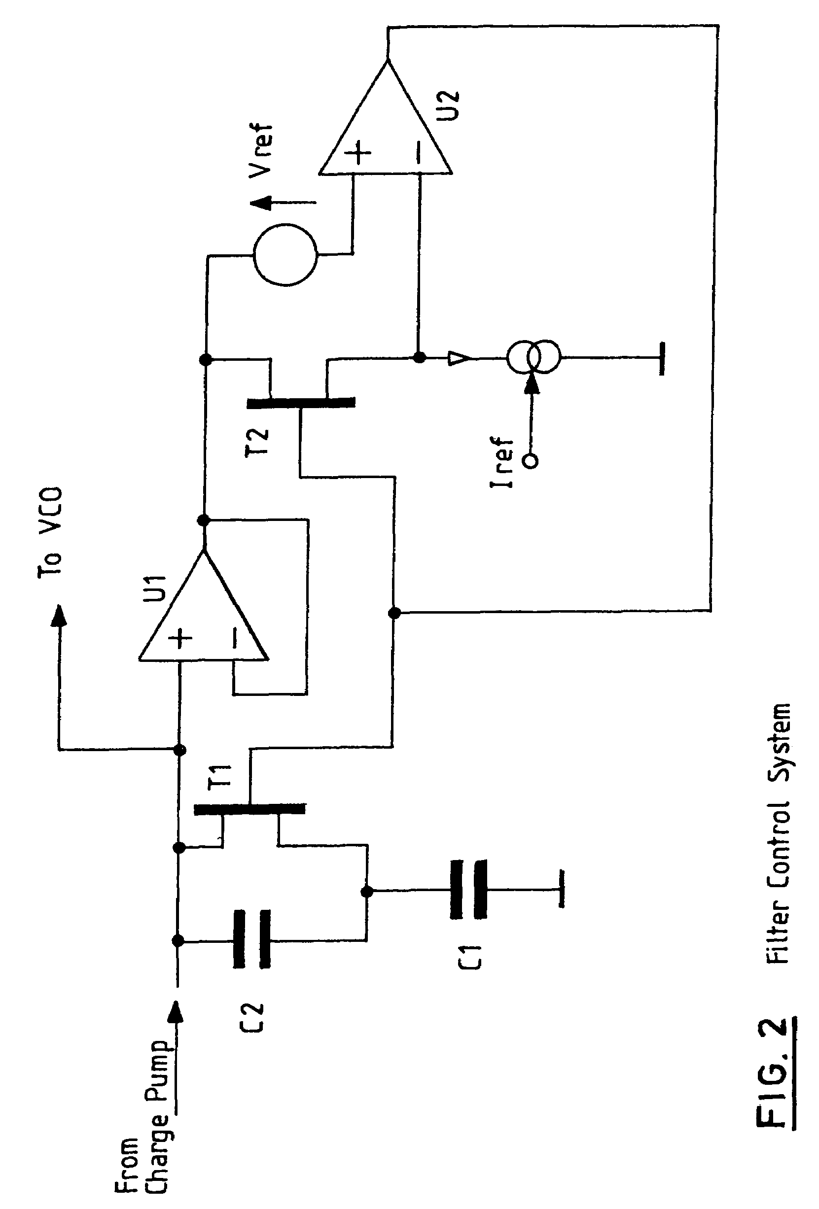
[0031]FIG. 2 shows the presently preferred embodiment of the present invention with a FET device, T1, being used to implement the active resistor element within a feedback system enabling accurate control of the resistance value. In this arrangement a voltage follower U1 is used to ‘bootstrap’ a reference FET device, T2, in the feedback control section to the filter voltage which is under the control of a voltage controlled oscillator (VCO). A current reference, Iref, which can be conveniently derived from the same source as that used to define the charge pump current in the PLL system, is used to define a voltage across T2. This voltage is then compared by an op-amp U2 to a reference voltage Vref and a feedback loop formed by U2 controls T2 (and subsequently T1) such that it simulates a resistance set by Vref / Iref. It is possible to control Iref or Vref to achieve continuous control of the resulting resistor value and therefore PLL filter response. This basic scheme can be used in ...
PUM
 Abstract
Description
Claims
Application Information