Nonvolatile semiconductor memory device including high efficiency and low cost redundant structure

a semiconductor memory and redundant structure technology, applied in semiconductor devices, digital storage, instruments, etc., can solve the problems of increasing the area for diverting wirings, the layout size cannot be reduced, and the cost of fabricating increases, so as to achieve stable and accurate reading of redundant information stored, low cost redundant relief, and high efficiency

Active Publication Date: 2007-01-16
RENESAS ELECTRONICS CORP
View PDF4 Cites 21 Cited by
  • Summary
  • Abstract
  • Description
  • Claims
  • Application Information

AI Technical Summary

Benefits of technology

[0021]Therefore, it is an object of the present invention to provide a nonvolatile semiconductor memory device which enables stable and accurate reading of redundant information stored in nonvolatile memories to realize high efficiency and low cost redundant relief.
[0023]With the nonvolatile semiconductor memory device according to the present invention, redundant information is stored in the nonvolatile memories constituting the program circuit, and the redundant information is read through paths separated from those for the reading operation for the normal memory cells prior to the normal data reading operation to realize accurate and stable reading operation, enabling high efficiency and low cost redundant relief.

Problems solved by technology

Further, in the aforementioned tests, there may be a case where semiconductor memory devices to be tested have electric characteristics which are out of specs required for proper operations.
While the laser trimming method may ensure excellent fabrication quality, it has the following problems since it involves a laser blow process for programming.
The first problem is that the layout size can not be reduced since there are restrictions that the size of fuse element can not be reduced to be smaller than the spot diameter of the directed laser and that there must be a sufficient clearance in the layout for preventing influences of the thermal fuse blowing on the adjacent fuse element.
Increases in the chip area directly result in increases in the fabricating cost.
The second problem is that since wirings can not be run through the layers over the area in which the fuse element is provided, an area for diverting wirings is further required.
The third problem is that redundant substitution can not be performed for defections generated after a molding process.
Once the chip has been encapsulated into a mold package, a laser light ray can not be directed to the upper surface of the chip, and therefore programming can not be performed.
The fourth problem is that redundant substitution can not be performed for defections generated after programming.
Programming is performed by blowing out the fuse element by laser blowing, and therefore once the programming has been completed, programming can not be performed again even if a further defection is generated.
The fifth problem is that the laser programming requires a specific laser blowing device, thereby increasing the cost of the device.
The aforementioned problems may induce increases in the fabricating cost of the semiconductor device.
On the other hand, in nonvolatile semiconductor memory devices, new problems will be generated as follows.
This makes difficult to perform the reading operation for the PROM area using the same procedure as that for the data reading operation for the normal memory cell area, which is performed under a stable external power supply voltage and stable internal power supply voltage.

Method used


Image

  • Nonvolatile semiconductor memory device including high efficiency and low cost redundant structure
  • Nonvolatile semiconductor memory device including high efficiency and low cost redundant structure
  • Nonvolatile semiconductor memory device including high efficiency and low cost redundant structure

Examples


first embodiment

[0046

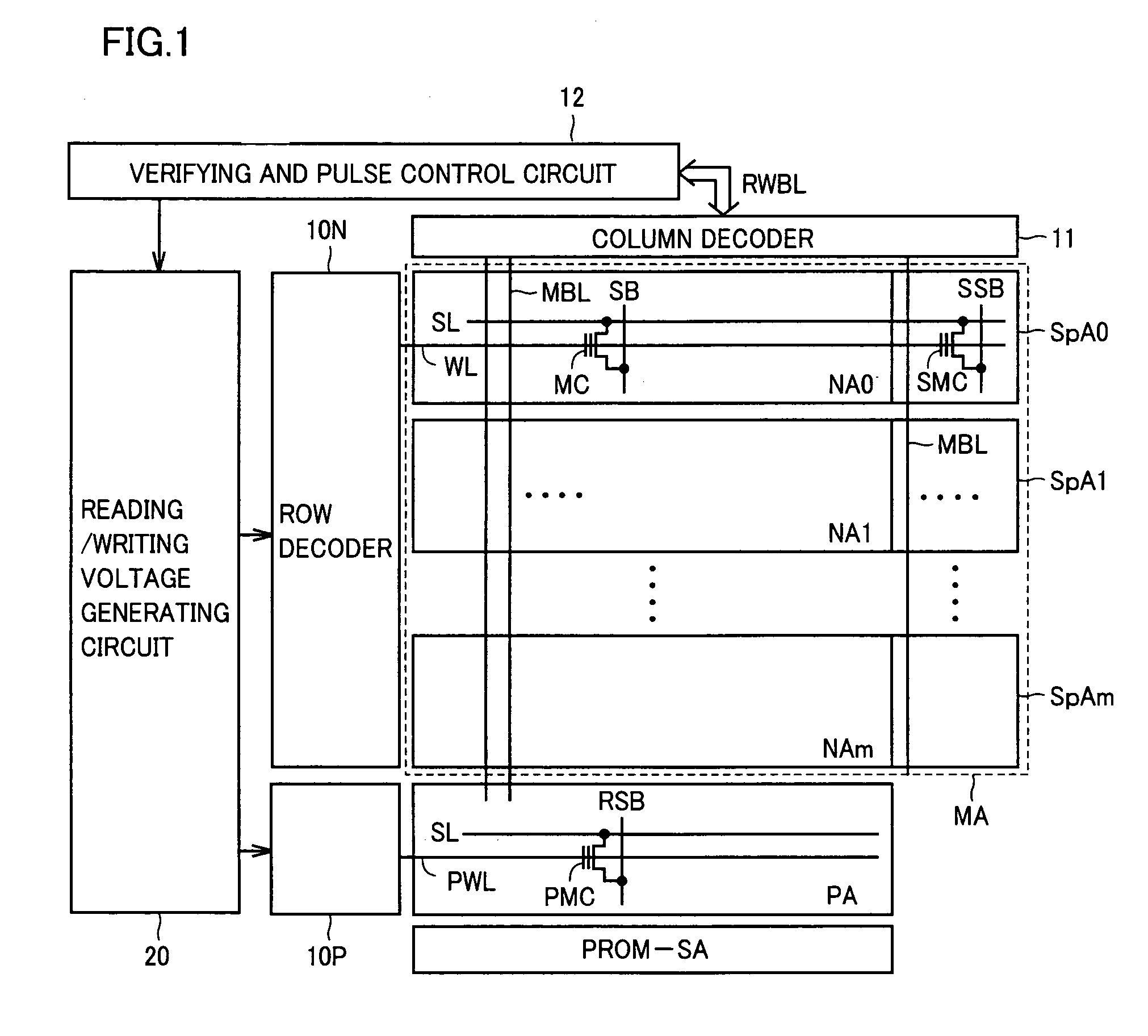
[0047]FIG. 1 is a schematic block diagram illustrating the structure of a nonvolatile semiconductor memory device according to the first embodiment of the present invention.

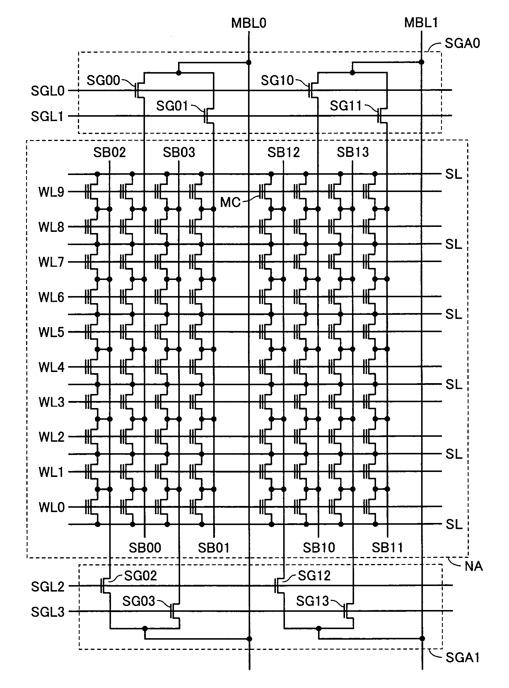
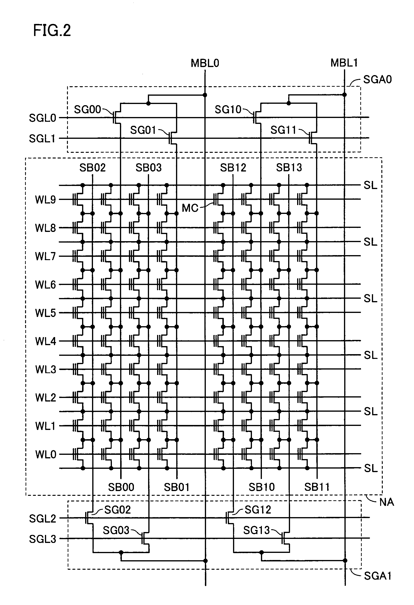
[0048]Referring to FIG. 1, the nonvolatile semiconductor memory device includes a memory array MA and a PROM area PA. The memory array MA includes normal memory cell areas NA0 to NAm (m is a natural number greater than 1) each including a plurality of normal memory cells (hereinafter, referred to as memory cells) MC placed in a matrix shape and redundant memory cell areas SpA0 to SpAm each including redundant memory cells SMC for relieving memory cells having a defect. The PROM area PA includes PROM (Programmable Read Only Memory) cells PMC as program circuits for nonvolatily storing redundant information such as address information identifying defective memory cells. Hereinafter, normal memory cell areas NA0 to NAm and redundant memory cell areas SpA0 to SpAm will be comprehensively represented by the chara...

second embodiment

[0113

[0114]In the first embodiment, there has been suggested a structure in which the reading of redundant information for PROM area PA is performed in paths separated from those for the reading for normal memory cell areas NA. Here, as previously described, the data reading operation for PROM area PA is performed at power-on. Therefore, stable reading operation is required, even though it is performed under unstable power supply voltage conditions.

[0115]In the present embodiment, there will be suggested a structure for stabilizing the reading operation for PROM area PA.

[0116]Generally, in the data reading operation for normal memory cell areas NA, as illustrated in FIG. 3, when the voltages of selected word lines WL have been raised to a predetermined internally-generated voltage VBOOST, the drain currents flowing through the memory cells MC to be read are read through the corresponding main bit lines MBL to determine whether the retained data is “0” or “1”.

[0117]For example, in a ...

third embodiment

[0136

[0137]In the second embodiment, there has been described a structure for setting the erasing threshold voltage of PROM cells PMC to a value lower than the erasing threshold voltage of memory cells MC in order to ensure a reading margin.

[0138]However, since the lower limit value of the threshold voltage is set to a value lower than that for memory cells MC, PROM cells PMC in the data-erased stage (“1” data-retaining state) have a low threshold voltage and therefore may become depression-type transistors which generate a drain current even when the gate voltage is 0 V. Accordingly, even when the gate voltage of a PROM cell PMC is 0 V, namely when the PROM cell PMC is in the non-selected state, a leak current (hereinafter, referred to as an off current) may be generated in the PROM cell PMC.

[0139]In the data reading for PROM area PA, the voltage level of only a single selected program word line PWL of the plurality of program word lines PWL is changed to a lower voltage VLOW than ...


PUM


Abstract

The PROM area is adjacent to the normal memory cell area. The data writing (normal writing) and the data reading (normal reading) for normal memory cell areas and the data writing (redundant writing) for the PROM area are carried out from the side of the normal memory cell areas. The data reading (redundant reading) for the PROM area is carried out from the side of the PROM area. In the PROM area, the PROM cells having the same structure as that of the normal memory cells are connected to the redundant sub bit lines. In the redundant writing, in the select gate area, the redundant sub bit lines and main bit lines are connected. In the redundant reading, in the redundant gate area having the same layout as that of the select gate area, the redundant sub bit lines are connected to redundant bit lines.

Description

BACKGROUND OF THE INVENTION[0001]1. Field of the Invention[0002]The present invention relates to a nonvolatile semiconductor memory devices and, more particularly, to a nonvolatile semiconductor memory device including a redundant structure.[0003]2. Description of the Background Art[0004]Semiconductor memory devices (hereinafter, referred to as semiconductor memories or semiconductor memory chips) are tested for proper operation after the fabricating processes have been completed and prior to shipment, and as the results of such tests, devices capable of proper operations are sorted out from defective devices.[0005]In such tests, even if there partially exists a defective circuit portion, the defective portion is substituted with a specific defective-portion substituting circuit to eliminate the defection and then fine adjustments for ensuring proper operation (hereinafter, referred to as trimming) are made. In general, such a defective-portion substituting circuit is referred to as...

Claims


Application Information

Patent Timeline
Patent Type & Authority Patents(United States)
IPC IPC(8): G11C11/34G11C16/06G11C16/14G11C29/00G11C29/04H01L27/105H01L27/115H01L31/113
CPCH01L27/115G11C29/82H01L27/105G11C29/789G11C16/04G11C17/14H10B69/00G11C29/00G11C16/14
Inventor HAMAMOTO, TAKESHIMITANI, HIDENORIOGURA, TAKU
Owner RENESAS ELECTRONICS CORP
Why Eureka
Try Eureka