Anisotropic film manufacturing

a technology of anisotropy and film, applied in the field of anisotropy films, can solve the problems of limiting the possibilities of using such crystals as substrates for epitaxial growth, limiting the number of single crystal materials suited for epitaxial growth, etc., to achieve the effect of simplifying the method of manufacturing, and reducing the number of substrates

Active Publication Date: 2007-01-23
NITTO DENKO CORP
View PDF24 Cites 22 Cited by
  • Summary
  • Abstract
  • Description
  • Claims
  • Application Information

AI Technical Summary

Benefits of technology

[0023]Technical result of the disclosed invention is the broadening of the functional possibilities of application of the anisotropic films while simplifyi...

Problems solved by technology

There are several disadvantages inherent in inorganic single crystals, which limit the possibilities of using such crystals as substrates for epitaxial growth.
In particular, the number of single crystal materials suited for epitaxial growth is rather restricted because the crystal surface can be reactive, and/or covered with oxides, and/or contain adsorbed water molecules.
The substrate can be nontransparent, possess undesired electronic and/or thermal properties, and so on.
Another restriction is the size of single crystal substrate that is available for reasonable cost.
Most of single crystals are produced in limited sizes and at high expense.
Despite all advantages of said known method, it is not free of significant drawbacks.
In particular, before growing an organic epitaxial layer possessing a desired orientation of planar organic molecules and required crystallographic parameters, in the general case, it is necessary to apply an alignment layer onto the substrate, which is an independent difficult task.
This circumstance may also present a certain disadvantage.
Any breakdowns in the temperature and vacuum regime lead to the appearance of defects in the growing layer, whereby both crystall...

Method used


Image

  • Anisotropic film manufacturing
  • Anisotropic film manufacturing
  • Anisotropic film manufacturing

Examples


Embodiment Construction

[0038]As generally described the present invention, a further understanding can be obtained by reference to the specific preferred embodiments, which are provided herein for purposes of illustration only and are not intended to limit the scope of the appended claims.

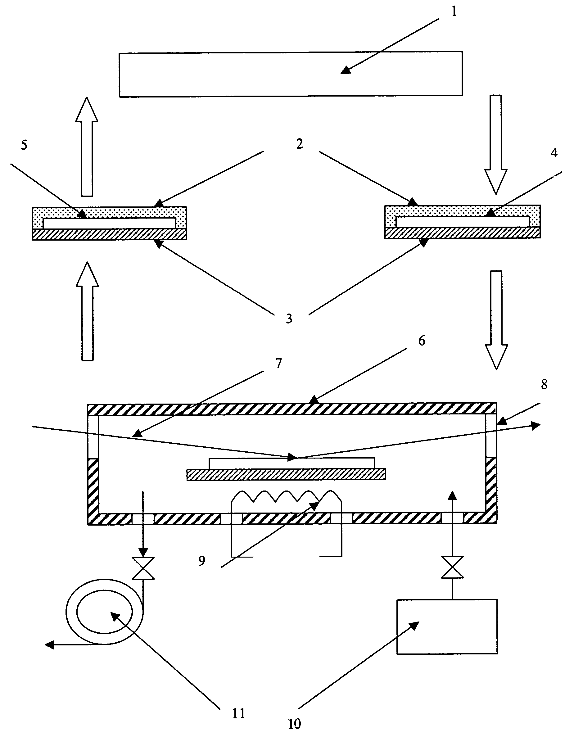
[0039]In one preferred embodiment, the disclosed invention provides a method for obtaining an anisotropic film. The first step of the method is providing a substrate. The second step is a deposition by means of Cascade Crystallization Process of at least one conjugated aromatic crystalline layer onto said substrate. The conjugated aromatic crystalline layer is characterized by the globally ordered crystalline structure with intermolecular spacing of 3.4±0.3 Å in the direction of one of the optical axes. The conjugated aromatic crystalline layer is formed by rodlike supramolecules, which comprise at least one polycyclic organic compound with conjugated π-system and ionogenic groups. The polycyclic organic compound can be ...


PUM


Abstract

The present invention relates to an anisotropic films and method for obtaining the same. The film comprises substrate and at least one modified conjugated aromatic crystalline layer deposited onto said substrate. The said layer is characterized by globally ordered crystalline structure with intermolecular spacing of 3.4±0.3 Å along one of optical axes. The modified conjugated aromatic crystalline layer is formed by rodlike supramolecules, which comprise at least one polycyclic organic compound with conjugated π-system. At least part of the modified conjugated aromatic crystalline layer has electric conductivity and is slightly soluble or insoluble in polar solvents. The films are useful in optical applications, such as polarizers and retarders, and in electronic and light emitting devices, such as fiber optics modulators and switches, solar cells, charge-coupled device (CCD), thin film transistor integrated circuits, light emitting diodes, and light emitting displays. The invention features the use of organic compounds for manufacturing thin crystal films useful in various applications.

Description

CROSS REFERENCE TO RELATED APPLICATIONS[0001]This application claims the benefit of the priority of U.S. Provisional Patent Application No. 60 / 440,939 filed Jan. 17, 2003, the disclosure of which is hereby incorporated by reference in its entirety.FIELD OF THE INVENTION[0002]The present invention relates to anisotropic films of organic aromatic compounds with flat, disk-shaped molecular structure (discotic molecules) that are useful in optical applications, such as polarizers and retarders, and in electronic and light emitting devices, such as fiber optics modulators and switches, solar cells, charge-coupled device (CCD), thin film transistor integrated circuits, organic light emitting diodes, and light emitting displays.[0003]The invention features the use of organic compounds for manufacturing thin anisotropic crystal films useful in various applications.BACKGROUND OF THE INVENTION[0004]The state of the art in oriented crystalline film manufacturing is known as epitaxial growth. T...

Claims


Application Information

Patent Timeline
IPC IPC(8): C30B29/54C09K19/52G02B5/30
CPCC09K19/52C09K2019/0496G02B5/3083G02B5/3033C09K2219/03Y10T428/31504
Inventor LAZAREV, PAVEL I.NAZAROV, VICTOR V.
Owner NITTO DENKO CORP
Why Eureka
Try Eureka