Apparatus for oscillating a head and methods for implementing the same

a head and head technology, applied in the field of cleaning semiconductor substrates, can solve the problems of deleterious defects in the processing of wafers, affecting the performance of integrated circuit devices, and certain shortcomings

Inactive Publication Date: 2007-01-30
LAM RES CORP
View PDF28 Cites 17 Cited by
  • Summary
  • Abstract
  • Description
  • Claims
  • Application Information

AI Technical Summary

Benefits of technology

[0020]Other aspects and advantages of the invention will become apparent from the following detailed description, taken in conjunction with the accompanying drawings, illustrating by way of example the principles of the invention.

Problems solved by technology

Particulate contaminants should be removed from wafer surfaces as the existence of such contaminants can have a detrimental effect on the performance of the integrated circuit devices.
Cleaning the front side (i.e., the active side or top surface) of wafers has traditionally been given a higher priority in typical wafer cleaning systems and processes because particulate contaminants adhered to the active side of a wafer can cause deleterious defects in the processing of the wafer.
However, as wafer sizes have increased and / or feature sizes have decreased, certain shortcomings have been associated with the failure to adequately and properly clean and process the backside (i.e., non-active side) of wafers.
As a result, the wafer surface is (locally) tilted or distorted, thus creating a focal plane deviation.
Although such deviation can be very slight, nonetheless, a number of challenges surface during photolithographic processes designed to form very small features.
Furthermore, the backside contaminants can undesirably migrate from one process tool / step thus contaminating subsequent processes.
Unfortunately, processing the front and backside of the wafer using the roller type and rotary type brushes can have certain disadvantages.
With respect to roller type brushes, fluid defined at the edge of the wafer can migrate to the opposite surface of the wafer as the rollers rotate, contaminating the otherwise cleaned surface.
The fluid migration phenomenon particularly hinders processing of a wafer wherein divergent process chemistries should be implemented.
However, due to fluid migration phenomenon, cleaning wafer surface by using truly divergent chemistries may not be achieved.
Irrespective of the brush type, expelled or migrated fluid droplets can contaminate the otherwise clean wafer surfaces, thus decreasing the quality of the cleaning operation.
Furthermore, fluid droplets can be expelled onto and around the cleaning chamber, reducing the reliability of the cleaning environment.
Still further, fluid migration can damage semiconductor devices on the wafer front side generating faulty wafers, thus reducing throughput.

Method used


Image

  • Apparatus for oscillating a head and methods for implementing the same
  • Apparatus for oscillating a head and methods for implementing the same
  • Apparatus for oscillating a head and methods for implementing the same

Examples


Embodiment Construction

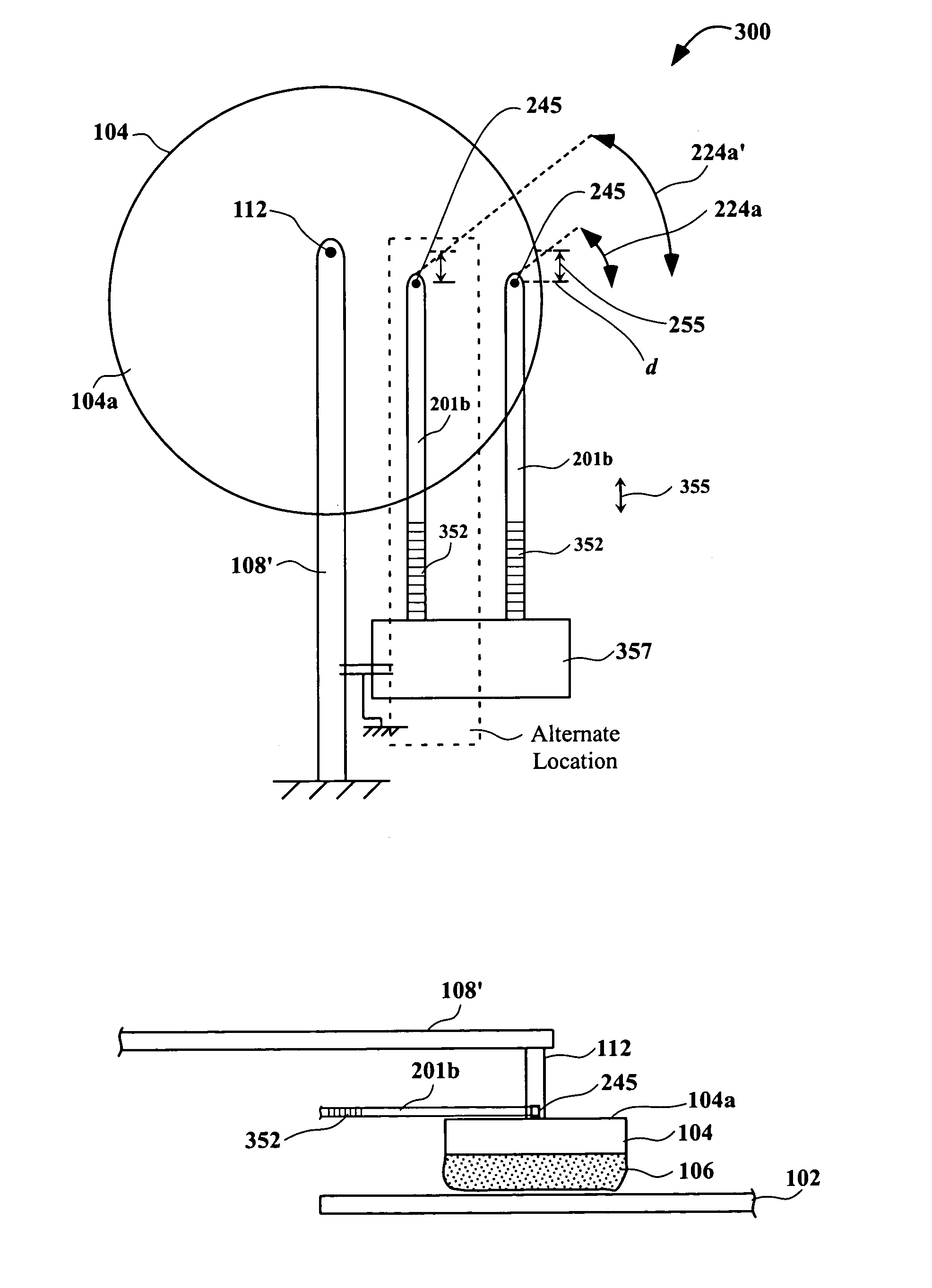
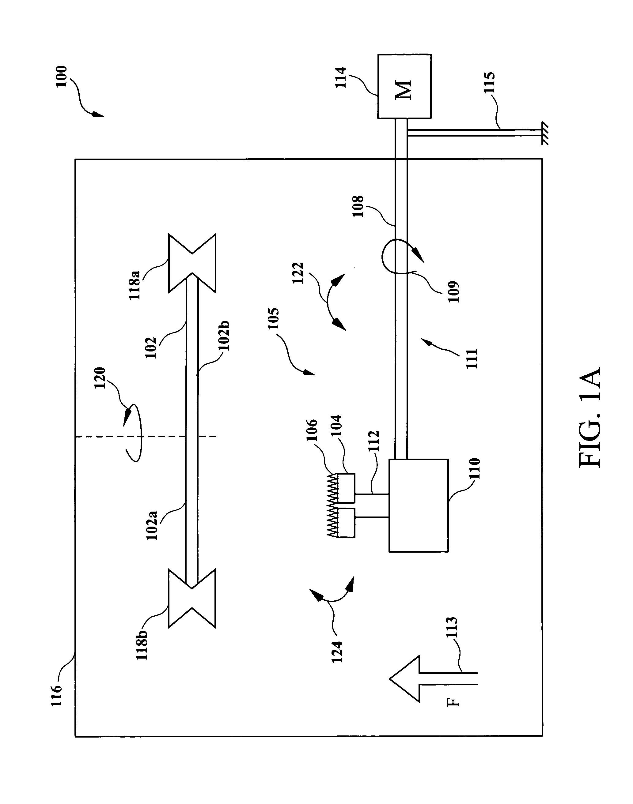
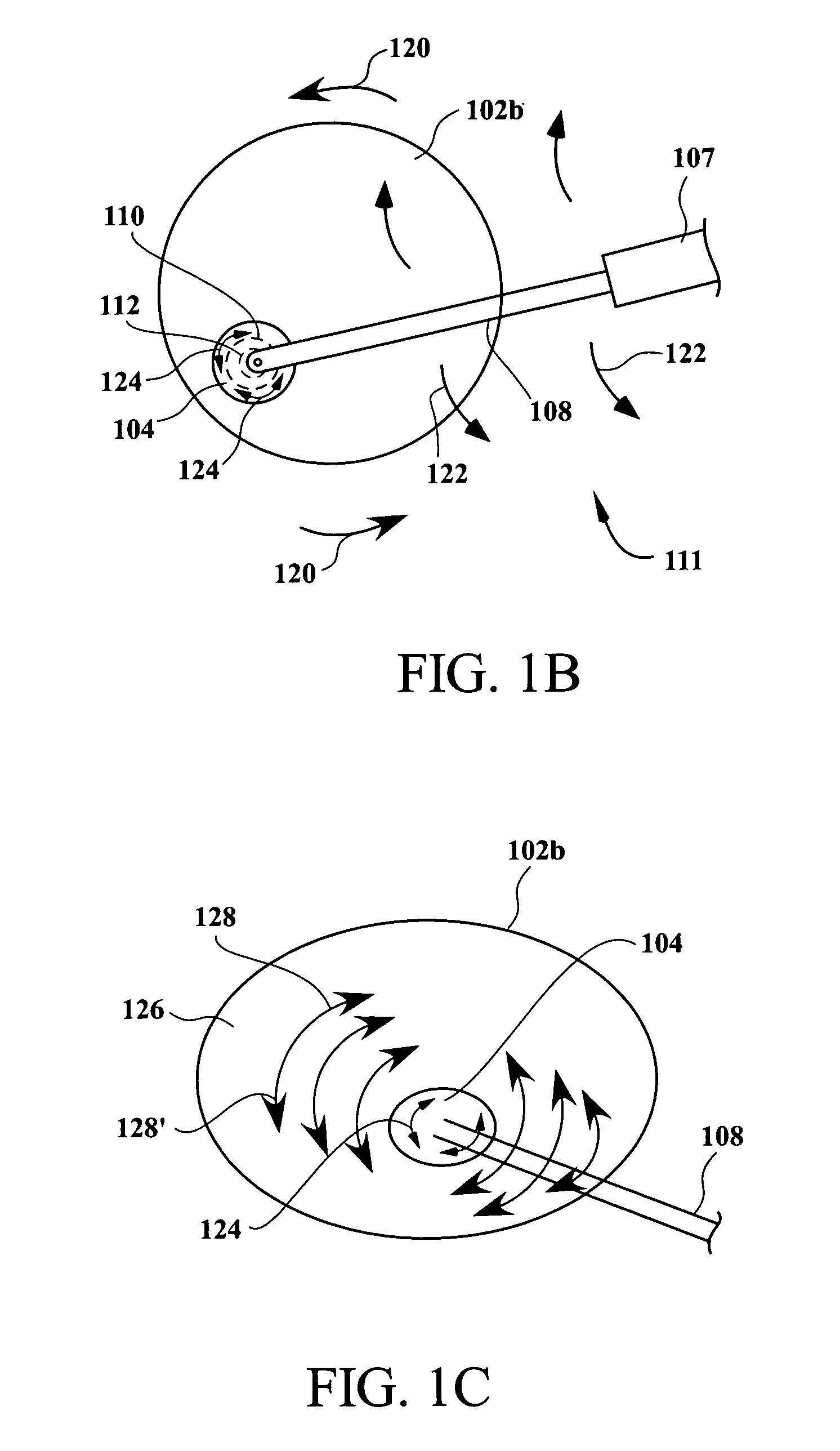
[0041]An invention capable of substantially reducing the fluid migration phenomenon and expelling of fluid droplets while enhancing efficiency and reliability of a cleaning operation is provided. In one embodiment, a wafer surface is cleaned as a brush secured to a head is applied onto the wafer surface while the head oscillates at a set frequency. In one embodiment, the backward and forward movements of the head creates an alternating pressure field on the wafer surface that is believed to improve the local mass transport of fluid under the brush thus enhancing the dislodging of particulate contaminants from wafer surfaces. The head can be made to oscillate by a mechanical actuator, a solenoid, or megasonic transducers. In one example, the head is designed to move across the wafer in any desired path. In one instance, the head can be moved across the wafer radially.

[0042]In the following description, numerous specific details are set forth in order to provide a thorough understandi...


PUM

PropertyMeasurementUnit
sizeaaaaaaaaaa
sizeaaaaaaaaaa
sizeaaaaaaaaaa

Abstract

An apparatus for brushing a surface of a substrate is provided. The apparatus includes a brush for scrubbing the surface of the substrate, a head for holding the brush, and an arm. The arm is configured to hold the head about a connection point. The arm is connected to an oscillating mechanism configured to cause the head to oscillate at an angle of rotation about the connection point.

Description

BACKGROUND OF THE INVENTION[0001]1. Field of the Invention[0002]The present invention relates generally to the fabrication of semiconductor devices and, more particularly, to cleaning semiconductor substrates.[0003]2. Description of the Related Art[0004]The fabrication of semiconductor devices involves numerous processing operations. These operations include, for example, impurity implants, gate oxide generation, inter-metal oxide depositions, metallization depositions, photolithography patterning, etching operations, chemical mechanical polishing (CMP), etc. As these operations generate particles and residues, wafer surfaces need to be cleaned so as to remove particulate contaminants adhered to the surfaces of the wafer.[0005]Particulate contaminants generally consist of tiny bits of distinctly defined material having an affinity to adhere to the surface of the wafer. Examples of particulate contaminants can include organic and inorganic residues, such as silicon dust, silica, slur...

Claims


Application Information

Patent Timeline
Patent Type & Authority Patents(United States)
IPC IPC(8): H01L23/58B08B6/00C25F1/00
CPCA46B13/04H01L21/67046H01L21/02057B08B1/04A46B2200/3086
Inventor TREUR, RANDOLPH E.BOYD, JOHN M.ANDERSON, TOMDE LARIOS, JOHN
Owner LAM RES CORP
Why Eureka
Try Eureka