Element substrate and a light emitting device

a technology of light emitting device and element substrate, which is applied in the direction of static indicating device, electroluminescent light source, instruments, etc., can solve the problems of affecting the image quality of the light source, and the capacitor storage capacity of the capacitor is increased, and the effect of enhancing the image quality

Inactive Publication Date: 2007-02-06
SEMICON ENERGY LAB CO LTD
View PDF67 Cites 46 Cited by
  • Summary
  • Abstract
  • Description
  • Claims
  • Application Information

AI Technical Summary

Benefits of technology

[0009]A transistor using polysilicon has high field effect mobility and large on-current. Therefore, it is suited for a light emitting device. However, the transistor using polysilicon has problems in that it is likely to have variations in characteristics due to a defect in a crystal grain boundary.
[0012]It is apparent from formula 1 that the drain current Ids of the driving transistor 701 in the saturation region is easily fluctuated even by small variations in the gate-source voltage Vgs. Therefore, it is necessary to keep the gate-source voltage Vgs, which is stored between the gate and the source of the driving transistor 701, not to be varied while the light emitting element 701 emits light. Thus, storage capacity of the capacitor 702 which is disposed between the gate and the source of the driving transistor 701 is required to be increased, and off-current of the switching transistor 700 and of the erasing transistor 708 is required to be suppressed low.
[0013]It is quite difficult to suppress off-current of the switching transistor 700 and of the erasing transistor 708 low while increasing on-current of the erasing transistor 708 for charging large capacitance in the formation process of the transistor.
[0015]In view of the foregoing problems, the invention provides a light emitting device and an element substrate which are not easily influenced by a parasitic capacitance and capable of suppressing variations in luminance intensity of the light emitting element 703 among pixels due to characteristic variations of the driving transistor 701 without suppressing off-current of the switching transistor 700 and of the erasing transistor 708 low and increasing storage capacity of the capacitor 702.
[0018]According to the invention, current flowing in a light emitting element is not influenced even without increasing storage capacity of a capacitor which is disposed between the gate and the source of the current controlling transistor or suppressing off-current of the switching transistor low. In addition, it is not influenced by the parasitic capacitance on the gate of the current controlling transistor either. Therefore, cause of variation is decreased, and image quality is thus enhanced to a great extent.
[0019]In addition, as there is no need to suppress off-current of the switching transistor low, manufacturing process of the transistor can be simplified, thus contributes greatly to the cost reduction and improvement in yield.

Problems solved by technology

However, the transistor using polysilicon has problems in that it is likely to have variations in characteristics due to a defect in a crystal grain boundary.

Method used


Image

  • Element substrate and a light emitting device
  • Element substrate and a light emitting device
  • Element substrate and a light emitting device

Examples


embodiment mode 1

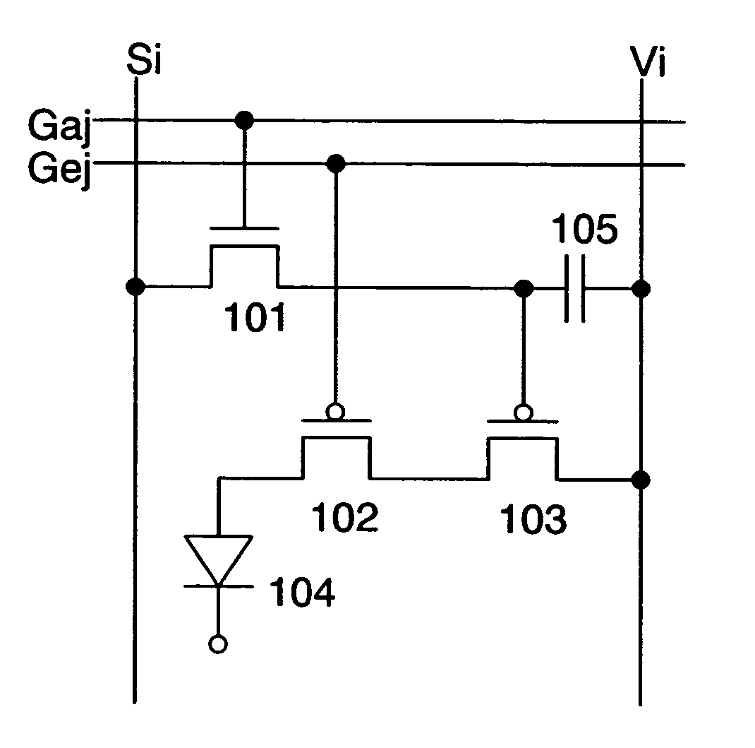
[0034]FIG. 1 shows an embodiment mode of a pixel of the light emitting device of the invention. The pixel shown in FIG. 1 comprises a light emitting element 104, a switching transistor 101 used as a switching element for controlling an input of a video signal to the pixel, a driving transistor 102 for controlling current flowing in the light emitting element 104, and a current controlling transistor 103 for controlling a current supply to the light emitting element 104. In addition, it is also possible to dispose in the pixel a capacitor 105 for storing a potential of a video signal.

[0035]The driving transistor 102 and the current controlling transistor 103 have the same conductivity. According to the invention, the driving transistor 102 is operated in a saturation region and the current controlling transistor 103 is operated in a linear region.

[0036]The channel length (L) of the driving transistor 102 may be longer than its channel width (W), and L of the current controlling trans...

embodiment 1

[0058]Described in this embodiment are a configuration of an active matrix display device to which the pixel configuration of the invention is applied and its drive.

[0059]FIG. 8 shows a block diagram of an external circuit and a schematic view of a panel.

[0060]An active matrix display device shown in FIG. 8 comprises an external circuit 8004 and a panel 8010. The external circuit 8004 comprises an A / D converter unit 8001, a power supply unit 8002, and a signal generator unit 8003. The A / D converter unit 8001 converts an image data signal which is input as an analog signal into a digital signal (video signal), and supplies it to a signal driver circuit 8006. The power supply unit 8002 generates power having a predetermined voltage from the power supplied from a battery or an outlet, and supplies it to the signal driver circuit 8006, a first scan driver circuit 8007, a second scan driver circuit 8012, an OLED 8011, the signal generator unit8003, and the like. The signal generator unit...

embodiment 2

[0074]Described in this embodiment is a second scan driver circuit, which adopts a method for controlling a white balance by applying a different potential to a gate electrode of each driving transistor in the red, green, and blue pixels as described with reference to FIG. 3 in embodiment mode. FIG. 10 shows a block diagram of the second scan driver circuit of this embodiment, and FIG. 3 shows a pixel configuration of this embodiment.

[0075]The second scan driver circuit 8012 comprises a shift register 1002 including a plurality of stages of D-flip flops 1001, a level shifter 1003, a buffer 1004, and the like.

[0076]It is assumed that a clock signal (G-CK), an inverted clock signal (G-CKB), and a start pulse (G-SP) are input.

[0077]The buffers 1004 each connected to scan lines Gerj (j=1 to y), Gegj (j=1 to y), and Gebj (j=1 to y) are connected to different power supply lines. Specifically, the buffer to which the scan line Gerj is connected is connected to a power supply line R, the bu...


PUM


Abstract

A light emitting device and an element substrate which are capable of suppressing variations in the luminance intensity of a light emitting element among pixels due to characteristic variations of a driving transistor without suppressing off-current of a switching transistor low and increasing storage capacity of a capacitor. According to the invention, a driving transistor also serves as an erasing transistor and the driving transistor is operated in a saturation region. The gate of the driving transistor is connected to an erasing scan line and it can be selected whether or not to flow current by a potential of the erasing scan line. In addition, a current controlling transistor which operates in a linear region is connected in series to the driving transistor, thus a video signal transmitting a light emission or non-emission of a pixel is input to the gate of the current controlling transistor through a switching transistor.

Description

BACKGROUND OF THE INVENTION[0001]1. Field of the Invention[0002]The present invention relates to a light emitting device comprising a plurality of pixels each having a light emitting element and a means for supplying current to the light emitting element.[0003]2. Description of the Related Art[0004]Since a light emitting element emits light by itself, it is highly visible and does not require a back light which is needed in a liquid crystal display device (LCD). Therefore, it is suitably applied to thin devices and not restricted in viewing angle. Because of these advantages, a light emitting device having a light emitting element has recently been drawing attentions as an alternative display device to a CRT and an LCD. It is to be noted that a light emitting element in this specification indicates an element whose luminance is controlled by current or voltage, and it includes an OLED (Organic Light Emitting Diode) or an MIM electron source element (electron discharge element) and t...

Claims


Application Information

Patent Timeline
Patent Type & Authority Patents(United States)
IPC IPC(8): G09G3/32H01L51/50G09G3/20G09G3/30G09G5/00H01L27/32H05B33/14
CPCG09G3/3233G09G3/2022G09G3/3266G09G3/3291G09G2300/0426H01L27/3244G09G2300/0842G09G2300/0861G09G2300/0866G09G2310/0251G09G2300/0809H10K59/12
Inventor OSAME, MITSUAKIANZAI, AYAYAMAZAKI, YU
Owner SEMICON ENERGY LAB CO LTD
Why Eureka
Try Eureka