High-speed chip-to-chip communication interface

a communication interface and high-speed technology, applied in the direction of dc level restoring means or bias distortion correction, baseband system details, instruments, etc., can solve the problems of requiring too many pins, pins adding cost, and need for higher-speed integrated circuits, and achieve the effect of easy scalabl

Active Publication Date: 2007-02-20
RIVERSTONE NETWORKS +1
View PDF11 Cites 141 Cited by
  • Summary
  • Abstract
  • Description
  • Claims
  • Application Information

AI Technical Summary

Benefits of technology

[0009]In one embodiment, the transmitter includes a transmitter controller and a transmitter interface circuit. Likewise, the receiver includes a receiver controller and a receiver interface circuit. Logic circuits feed data to the transmitter controller synchronously with an internal clock. The transmitter interface circuit, controlled by the transmitter controller, interleaves the data and provides the interleaved data to the interconnect bus synchronously with transitions of a bus clock. The receiver interface circuit, controlled by the receiver controller, captures data from the interconnect bus, de-interleaves the captured data and resynchronizes the data to an internal clock of the receiver. To the logic feeding the transmitter and logic getting data from the receiver, the interconnect of the present embodiment appears to be simple digital pipeline where latency is dependent on the length of the signal traces connecting the transmitter and the receiver.
[0014]Embodiments of the invention are easily scalable. A single integrated circuit can implement multiple transmitters and multiple receivers. In one embodiment of the invention, sixteen transmitters and sixteen receivers, which can provide more than 25 Gb / s of bandwidth capacity, are implemented on a single chip.

Problems solved by technology

The explosive demands from the Internet are driving the need for higher speed integrated circuits.
But eventually, this solution runs into the problem of requiring too many pins.
Pins add cost: pins take board area, increase package costs and size, increase test costs and affect electrical performance.
Increasing bus width also makes length-matching signal traces, which is required in many high performance systems, more difficult.
Increasing bus clock frequency is effective but only to a point beyond which it becomes challenging to support reliable data transfer using standard printed circuit board (PCB) technology and standard manufacturing processes.
For instance, high frequency clock chips are expensive and difficult to build, and there is more electrical loss on the boards interconnecting the chips.
Other electromagnetic problems such as cross-talk are more likely to materially affect signal transmission at very high frequency.
Differential signaling technologies typically require complex circuitry that consumes large die areas and large amounts of power.
Furthermore, differential signaling technologies are difficult to implement because they often require one or more Phase-Locked Loops (PLL) or Delay-Locked Loops (DLL) as well as some additional complex analog circuits.
In addition, differential signaling technologies require careful isolation because they tend to be sensitive to core switching noise.

Method used


Image

  • High-speed chip-to-chip communication interface
  • High-speed chip-to-chip communication interface
  • High-speed chip-to-chip communication interface

Examples


Embodiment Construction

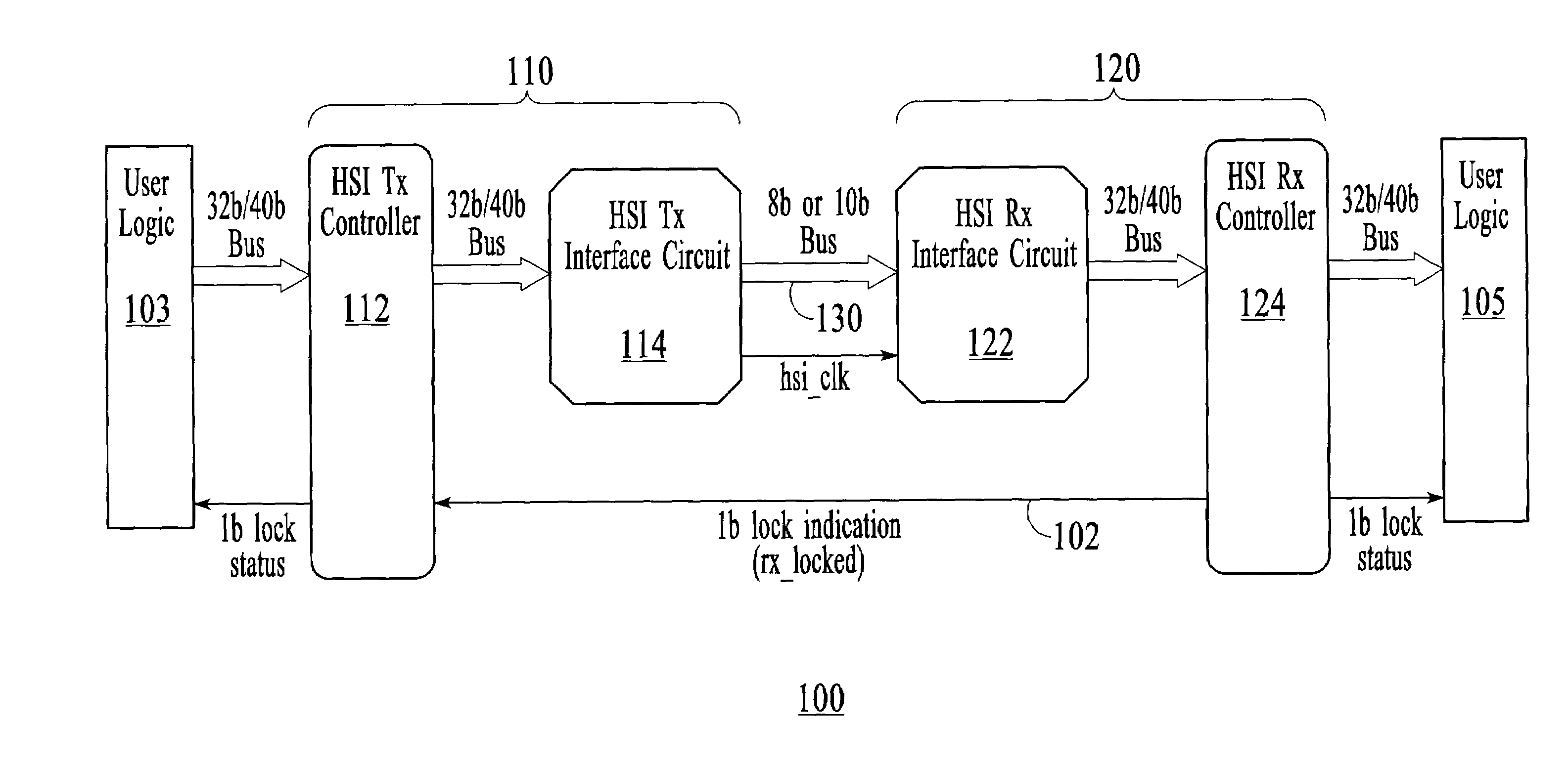
[0041]FIG. 1 is a block diagram illustrating a High-Speed Interconnect (HSI) link 100 for communicating data between chips in accordance with one embodiment of the invention. The HSI link 100 includes a transmitter 110 and a receiver 120 connected by an interconnect bus 130. In one embodiment, the transmitter 110 and the receiver 120 are implemented within separate chips (not shown) but within a same backplane of a high-speed electronic communication system. As shown, the transmitter 110 includes a HSI Tx Controller 112 and a HSI Tx Interface Circuit 114. The receiver 120 includes a HSI Rx Interface Circuit 122 and a HSI Rx Controller 124. The HSI Tx Interface Circuit 114 and the HSI Rx Interface Circuit 122 are preferably implemented as hard macro cells (or “hardmacs”), and the HSI Tx Controller 112 and the HSI Rx Controller 124 are preferably synthesizable. Also shown in FIG. 1 is user logic 103 that feeds data to the HSI Tx Controller 112 and user logic 105 that receives data fro...


PUM


Abstract

A high-speed parallel interface for communicating data between integrated circuits is disclosed. The interface is implemented by a transmitter and receiver pair and a single-ended parallel interconnect bus coupling to the transmitter and receiver pair. As opposed to transmitting small swing signals over differential signal lines, the transmitter transmits data to the receiver at full swing over the single-ended parallel interconnect bus. The invention can be implemented with simple CMOS circuitry that does not consume large die area. Accordingly, many link interfaces can be implemented on a single chip to provide a large data bandwidth.

Description

CROSS-REFERENCE TO RELATED APPLICATION[0001]This application is entitled to the benefit of provisional Patent Application Ser. No. 60 / 385,989, filed Jun. 4, 2002, and is related to co-pending non-provisional Patent Application entitled “HIGH-SPEED CHIP-TO-CHIP COMMUNICATION INTERFACE WITH SIGNAL TRACE ROUTING AND PHASE OFFSET DETECTION”, Serial Number (TBD), filed (TBD), Attorney Docket No. RSTN-028, both of which are hereby incorporated by reference.FIELD OF THE INVENTION[0002]The invention related generally to a high-speed chip-to-chip communication interface.BACKGROUND OF THE INVENTION[0003]A few years ago, a small number of people accessed primarily text-based information through the Internet. Today, motion video and sound combined with a huge increase in users have pushed the internet infrastructure and the performance of communications equipment to the limit. The explosive demands from the Internet are driving the need for higher speed integrated circuits. As the speed of inte...

Claims


Application Information

Patent Timeline
Patent Type & Authority Patents(United States)
IPC IPC(8): H04L27/00H04L25/00H04L25/06G06F13/14H04L7/00H04L7/04H04L25/02H04L25/45
CPCH04L7/005H04L25/45H04L7/0008H04L7/046H04L25/0292H04L25/028
Inventor KLEVELAND, BENDIKANDERSON, ERICAYBAY, GUNESFEROLITO, PHILIP
Owner RIVERSTONE NETWORKS
Why Eureka
Try Eureka