High-density plasma (HDP) chemical vapor deposition (CVD) methods and methods of fabricating semiconductor devices employing the same

a technology of high-density plasma and chemical vapor deposition, which is applied in the field of high-density plasma (hdp) chemical vapor deposition (cvd) methods and methods of forming semiconductor devices, can solve the problems and increasing the difficulty of narrowing. narrow, the effect of reducing the number of fluorine atoms

Inactive Publication Date: 2007-02-27
SAMSUNG ELECTRONICS CO LTD
View PDF10 Cites 232 Cited by
  • Summary
  • Abstract
  • Description
  • Claims
  • Application Information

AI Technical Summary

Benefits of technology

[0013]Embodiments of the present invention provide a method of improving gap fill capabilities and reducing the amount of fluorine atoms in gap-fill layers as compared to conventional HDP-CVD methods.
[0015]Accordingly, high aspect ratio gaps, e.g., trenches formed in a substrate are substantially completely filled with a dielectric without voids, using high-density plasma chemical vapor deposition (HDP-CVD) while significantly reducing fluorine atoms from the deposited insulation layer and the defects resulting therefrom.

Problems solved by technology

In particular, it has become increasingly difficult to fill narrow, high-aspect ratio gaps or recessed features due to the limitations of existing CVD techniques.
This is because most CVD processes tend to deposit more material on the upper region than on the lower region of gap sidewalls and to form undesirable overhangs at the entry of the gap.
As a result, the top portion of the high-aspect ratio gaps often closes prematurely leaving voids within the gaps.
Such gaps degrade the device characteristics, for example, by trapping undesirable impurities within the gaps.
This causes problems such as the formation of voids or reentrant features, e.g., a narrowing at the tops of the gaps.
These problems have become a major challenge for successful production of more highly-integrated advanced semiconductor devices.
However, the process disclosed in the '745 invention is very complicated and time-consuming, which leads to low throughput.
Further, with such conventional methods, gap-fill process margins are relatively narrow, with problems such as clipping (excessive etching) or voids within the filled gaps (excessive deposition).
However, conventional HDP-CVD methods using fluorine-containing gas tend to incorporate an undesirable number of fluorine atoms that significantly degrade the device characteristics.
For example, use of too many fluorine atoms can cause undesirable out-diffusion of fluorine atoms into the silicon substrate, delamination of layers and / or damage to silicon active regions.
Attempts to overcome this problem by using a barrier layer to prevent out-diffusion of the fluorine atoms understandably complicates the overall manufacturing process, decreases throughput, and increases manufacturing costs.

Method used


Image

  • High-density plasma (HDP) chemical vapor deposition (CVD) methods and methods of fabricating semiconductor devices employing the same
  • High-density plasma (HDP) chemical vapor deposition (CVD) methods and methods of fabricating semiconductor devices employing the same
  • High-density plasma (HDP) chemical vapor deposition (CVD) methods and methods of fabricating semiconductor devices employing the same

Examples


Embodiment Construction

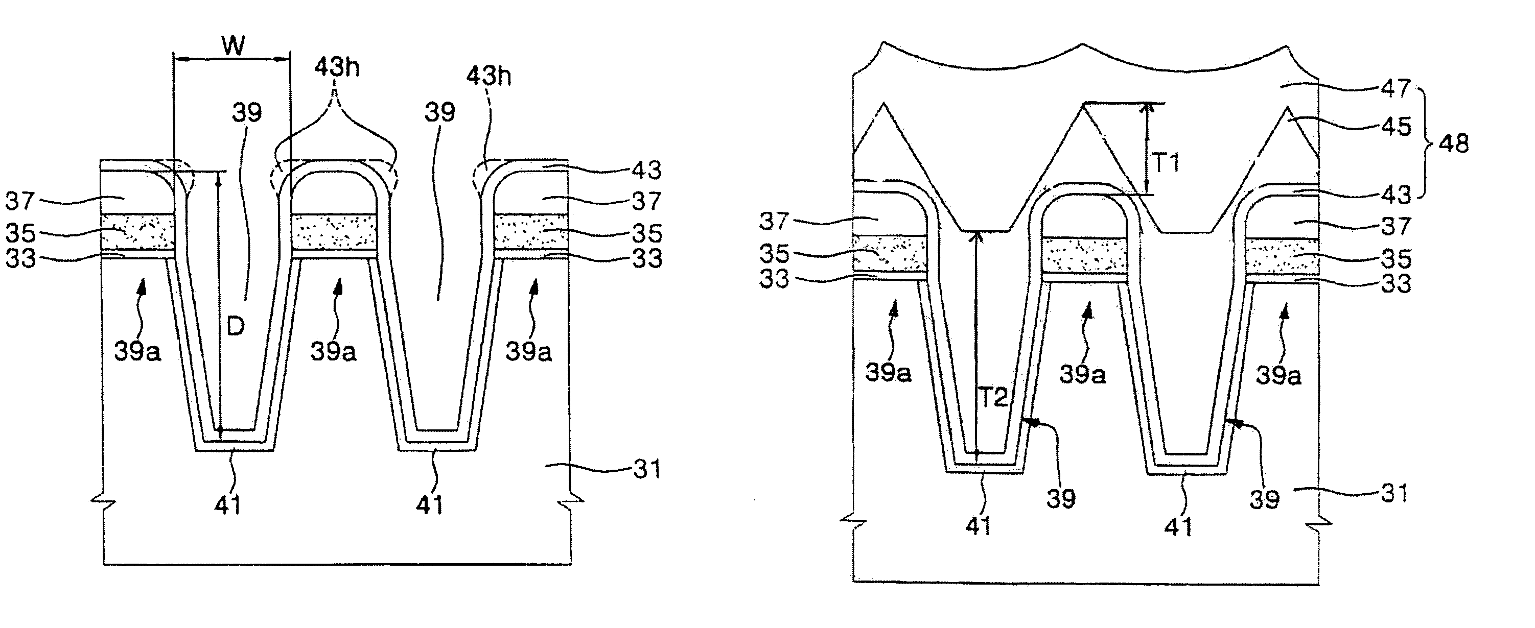
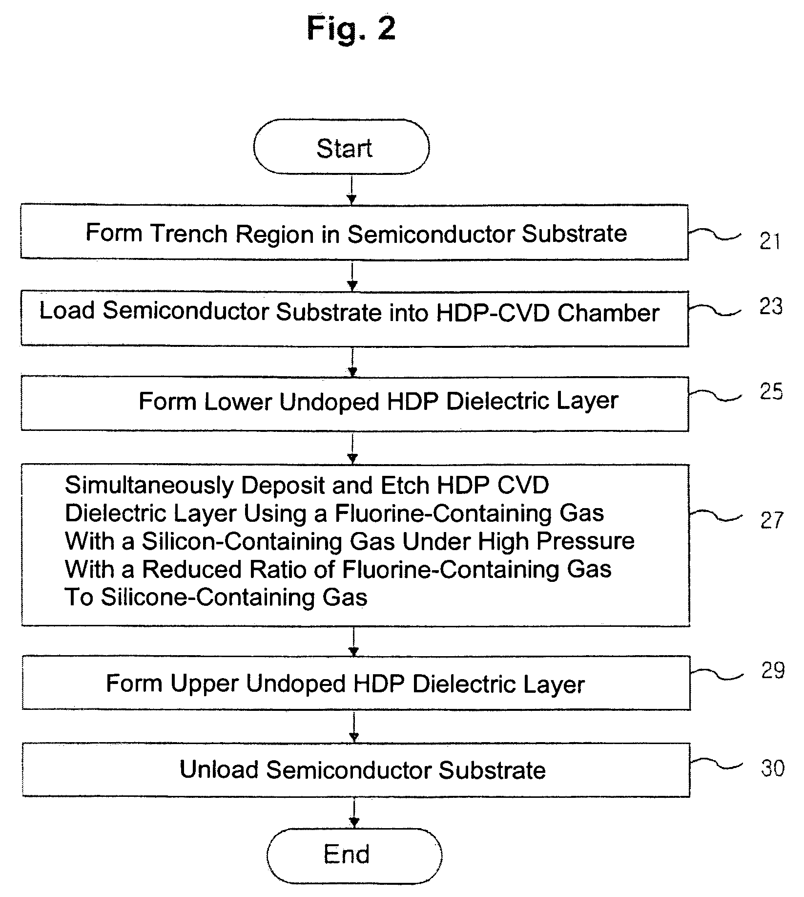
[0024]The present invention concerns the deposition of a dielectric layer using high density plasma (HDP) chemical vapor deposition (CVD) techniques. The deposited layer has improved gap-fill capabilities as compared to the prior art HDP CVD methods.

[0025]In the following description, numerous specific details are provided. However, one skilled in the relevant art will recognize that the invention can be practiced without one or more of the specific details, or with other methods, components, materials, etc. In other instances, well-known structures, materials, or operations are not shown or described in detail to avoid obscuring novel aspects of the invention.

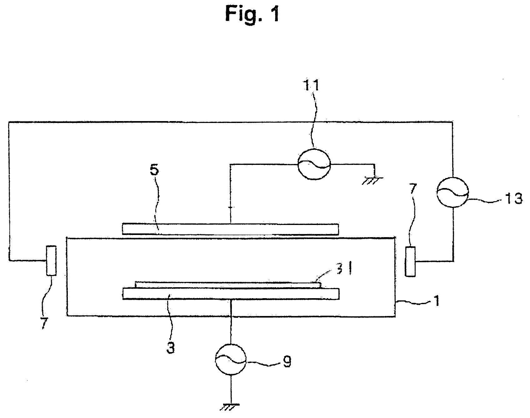
[0026]In general, HDP-CVD systems operate at lower pressure ranges (a few mTorr) than do low-density plasma systems. This is because such low pressure levels improve gap-fill results by increasing the mean free path of ions and dissociated species. This has been thought to increase the probability that such dissociated species...


PUM

PropertyMeasurementUnit
pressureaaaaaaaaaa
thicknessaaaaaaaaaa
thicknessaaaaaaaaaa

Abstract

In one embodiment, a semiconductor substrate is placed into a process chamber. A gas mixture including a silicon-containing gas, a fluorine-containing gas, an inert gas, and an oxygen gas is introduced into the chamber at a pressure range of from about 30 mTorr to about 90 mTorr. During this time, deposition and etching processes are concurrently performed using a plasma to form a high-density plasma (HDP) insulating layer on the semiconductor substrate. A ratio of deposition to etching is from about 3:1 to about 10:1. A ratio of a flow rate of the fluorine-containing gas to a flow rate of the silicon-containing gas is less than about 0.9.

Description

CROSS-REFERENCE TO RELATED APPLICATION[0001]The present application claims the priority of Korean Patent Application No. 2005-26185, filed Mar. 29, 2005 in the Korean Intellectual Property Office. The disclosures of all of the above applications are incorporated herein in their entirety by reference.BACKGROUND OF INVENTION[0002]1. Field of the Invention[0003]The present invention generally relates to the fields of semiconductor fabrication and, more particularly, to high-density plasma (HDP) chemical vapor deposition (CVD) methods and methods of forming semiconductor devices using the same.[0004]2. Description of Related Art[0005]For fabricating semiconductor devices, various processing steps are needed. In particular, chemical vapor deposition (CVD) processes are generally used to fill gaps such as spaces between adjacent raised structures such as transistor gates, conductive patterns, e.g. signal lines, trenches and the like with an insulating material.[0006]As semiconductor devic...

Claims


Application Information

Patent Timeline
Patent Type & Authority Patents(United States)
IPC IPC(8): H01L21/311
CPCC23C16/045C23C16/402C23C16/505H01L21/02131H01L21/02211H01L21/31629H01L21/02304H01L21/02362H01L21/02274H01L21/31608H01L21/31625A45D44/22
Inventor NAM, JEONG-HOONJEON, JIN-HO
Owner SAMSUNG ELECTRONICS CO LTD
Why Eureka
Try Eureka