Method of manufacturing an SOI wafer where COP's are eliminated within the base wafer

a technology of soi and base wafers, applied in the direction of basic electric elements, electrical apparatus, semiconductor devices, etc., can solve the problems of micro voids, and achieve the effects of reducing costs, improving yield, and improving inspection yield

Inactive Publication Date: 2007-03-06
SHIN-ETSU HANDOTAI CO LTD
View PDF33 Cites 18 Cited by
  • Summary
  • Abstract
  • Description
  • Claims
  • Application Information

AI Technical Summary

Benefits of technology

[0020]As described above, when the SOI wafer is produced by bonding the bond wafer to the base wafer via the insulator film and thinning the bond wafer, if an epitaxial wafer, an FZ wafer, a nitrogen doped wafer, a hydrogen annealed wafer, an intrinsic gettering wafer, a nitrogen doped and annealed wafer, or an entire N-region wafer is used as the base wafer, an SOI wafer that COPs hardly exist near a surface of the base wafer can be obtained. Therefore, even if the insulator film and the SOI layer are thinner, there is no case that many COPs due to the base wafer are detected in the inspection after the SOI wafer was completed, and thus measurements which precisely reflect the number of COPs in the SOI layer can be performed. And also, a high quality SOI wafer that generation of micro voids at an interface between the base wafer and the insulator film is suppressed can be produced.
[0031]Further, in such an SOI wafer, the SOI layer on which elements are formed can be precisely inspected to see whether it is good or bad before device fabrication, which can lead to improvement of device yield and reduction in production cost.

Problems solved by technology

In this case also, it was revealed that the COP did not exist in the SOI layer, but existed on a surface of the base wafer, and moreover, the insulator film and the base wafer could not be bonded in the region in which the COP existed, resulting in a micro void.

Method used


Image

  • Method of manufacturing an SOI wafer where COP's are eliminated within the base wafer
  • Method of manufacturing an SOI wafer where COP's are eliminated within the base wafer
  • Method of manufacturing an SOI wafer where COP's are eliminated within the base wafer

Examples


example 1

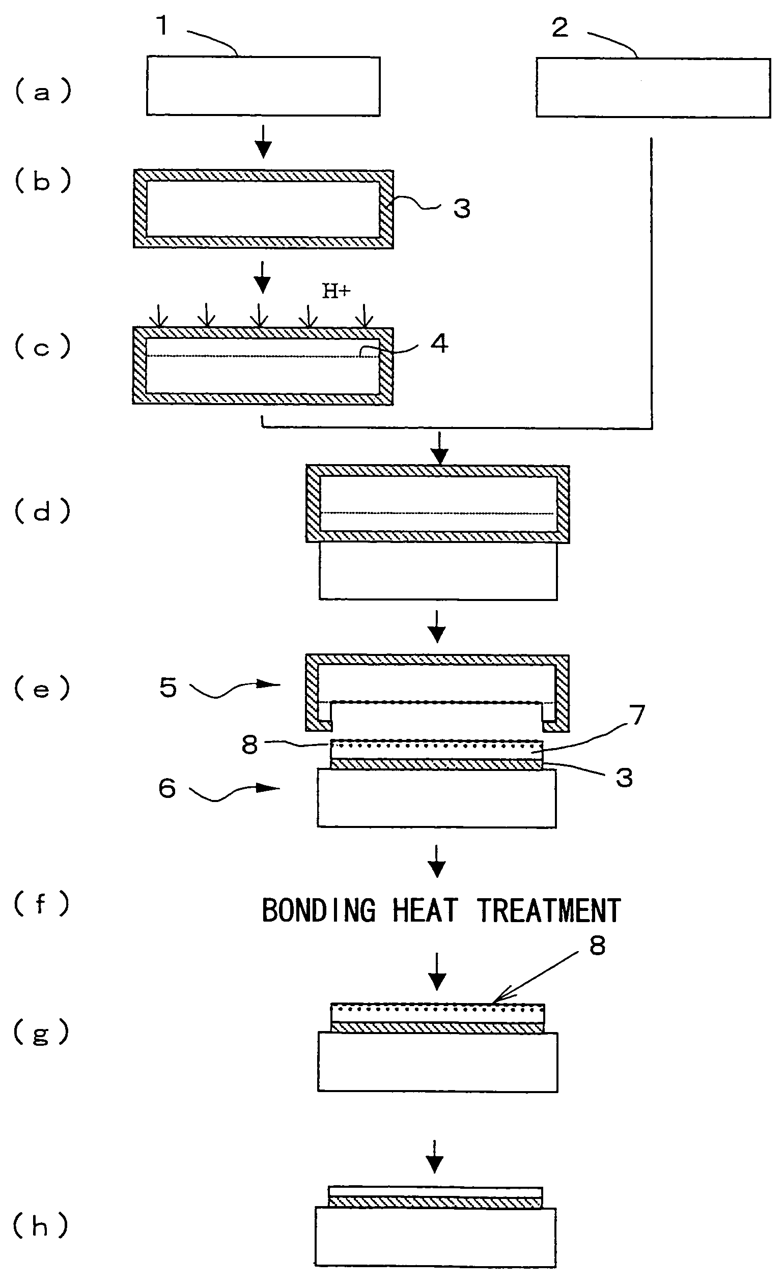
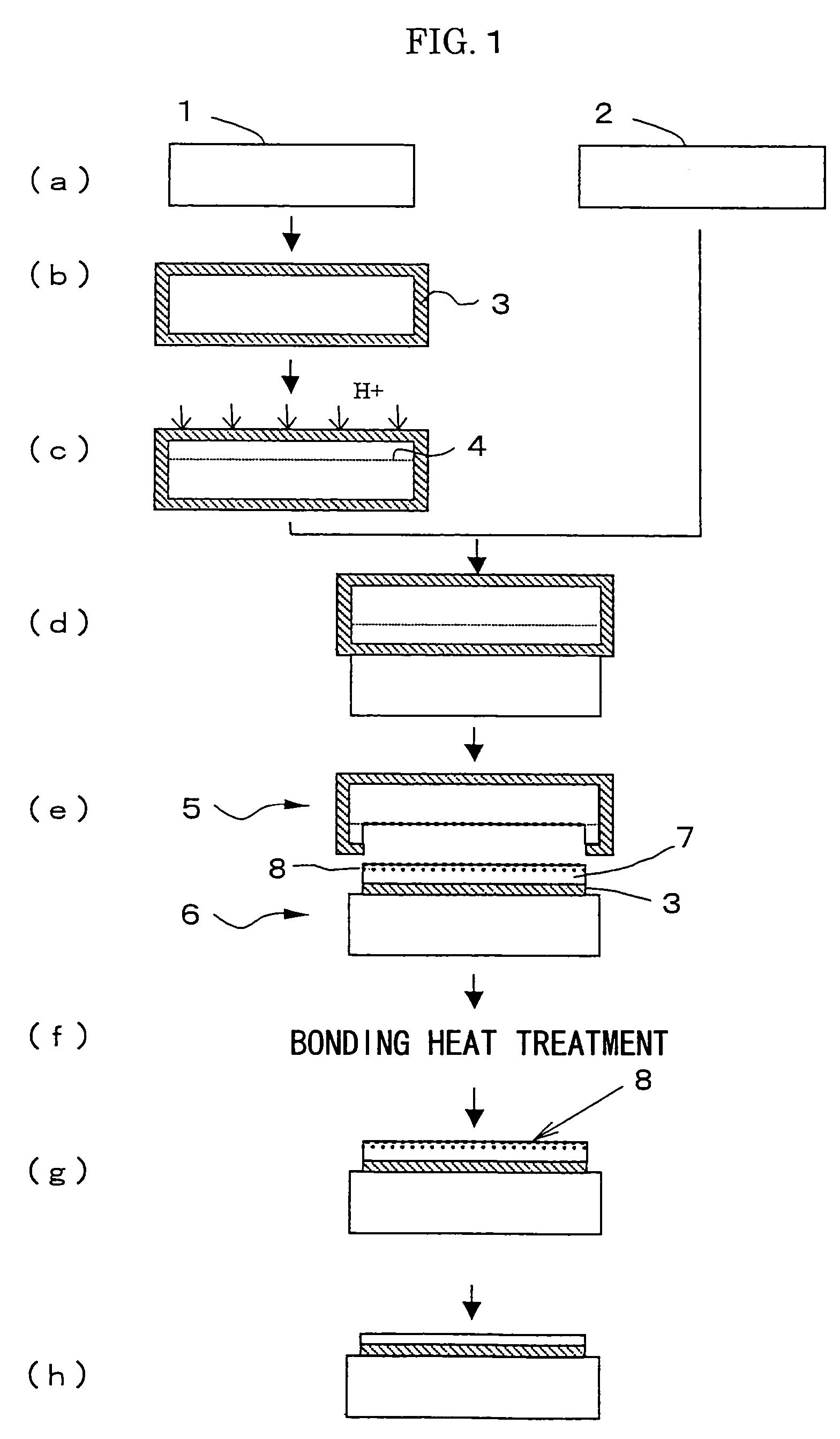
[0065]By using a so-called MCZ method in which a magnetic field is applied to a silicon melt, a silicon single crystal ingot was grown at a pulling rate of 1.8 mm / min. This silicon crystal ingot was processed into silicon wafers by slicing, etching, polishing, and the like, and wafers having a crystal orientation of , a conductivity type of P-type, a resistivity of 10 Ω·cm, and a diameter of 200 mm were produced.

[0066]The silicon wafers were subjected to a heat treatment using an RTA apparatus (Rapid Thermal Annealler: a rapid heating / rapid cooling apparatus, SHS-2800, manufactured by AST Corporation) under an atmosphere of 100% hydrogen, at 1200° C., for 10 seconds. In order to use the wafers as both a bond wafer and a base wafer, each surface to be bonded was polished with a stock removal of 10 nm so that haze and the like generated due to the heat treatment on the wafer surface were removed.

[0067]By using such a bond wafer and a base wafer, an SOI wafer of which SOI layer has a t...

example 2

[0074]A silicon single crystal ingot was grown under the same conditions as in Example 1 except that the ingot was doped with nitrogen of 1×10¹⁴ atoms / cm3. The single crystal ingot was processed into silicon wafers by slicing, etching, polishing, and the like, and thereby wafers having a crystal orientation of , a conductivity type of P-type, a resistivity of 10 Ω·cm, and a diameter of 200 mm were produced.

[0075]Such wafers are used as a bond wafer and a base wafer, and an SOI wafer was produced by the same processes and production conditions as in Example 1. And then, the number of COPs was observed by the particle counter as in Example 1.

[0076]As a result, the number of COPs observed on the wafer was 7 numbers / wafer. Also, when cross sections of points where the COPs exist were observed by the TEM, it was found that COPs generated on the base wafer were 4 numbers / wafer. However, micro voids did not exist therein.

example 3

[0077]The same crystal ingot as in Example 2 was processed into wafers by slicing, etching, polishing, and the like, and wafers having a crystal orientation of , a conductivity type of P-type, a resistivity of 10 Ω·cm, and a diameter of 200 mm were obtained.

[0078]Such silicon wafers were subjected to a heat treatment under an atmosphere of argon gas at 1200° C. for 1 hour. In order to use the wafers as both a bond wafer and a base wafer, each surface to be bonded was polished with a stock removal of 10 nm so that haze and the like generated due to the heat treatment on each wafer surface were removed.

[0079]By using the bond wafer and the base wafer, an SOI wafer was produced under the same processes and production conditions as in Example 1. And then, the number of COPs was observed by the particle counter as in Example 1.

[0080]As a result, the number of COPs observed on the wafer was 1 number / wafer. Also, when a cross section of the points where the COP exists was observed by the T...


PUM


Abstract

When an SOI wafer is produced by using a bond wafer made of silicon single crystal to form an SOI layer and a base wafer made of silicon single crystal to be a support substrate, one silicon wafer selected from a group consisting of an epitaxial wafer, an FZ wafer, a nitrogen doped wafer, a hydrogen annealed wafer, an intrinsic gettering wafer, a nitrogen doped and annealed wafer, and an entire N-region wafer is used as the bond wafer. Thereby, even where a thin insulator film or a thin SOI layer is formed in the SOI wafer, COPs are hardly detected in inspection of the SOI layer after the SOI wafer was completed, and a high quality SOI wafer is provided.

Description

TECHNICAL FIELD[0001]The present invention relates to an SOI (Silicon On Insulator) wafer suitable for semiconductor device fabrication.BACKGROUND ART[0002]An SOI wafer is produced as follows, for example. An insulator film such as an oxide film (Box layer, which is to become a buried oxide film (insulator film)) is formed on at least one of a first silicon wafer (hereafter, called “bond wafer”, from which an SOI layer is formed) having at least one flattened and mirror-polished main surface and a second silicon wafer (hereafter, called “base wafer”, which is to become a support substrate). Each main surface of the two silicon wafers is bonded and joined to each other via the insulator film. After the wafers are subjected to a heat treatment to firmly join them, the other main surface opposite to the bonded main surface of the bond wafer is ground and polished to have a predetermined thickness, and thereby an SOI layer (an element fabrication layer) is formed on the insulator film, ...

Claims


Application Information

Patent Timeline
Patent Type & Authority Patents(United States)
IPC IPC(8): H01L21/30H01L21/02H01L21/322H01L21/762H01L27/12
CPCH01L21/76254H01L21/3225H01L21/3226
Inventor NAKANO, MASATAKE
Owner SHIN-ETSU HANDOTAI CO LTD
Why Eureka
Try Eureka