Semiconductor storage device, semiconductor device, manufacturing method of semiconductor storage device, and mobile electronic device

a semiconductor storage and semiconductor technology, applied in semiconductor devices, digital storage, instruments, etc., can solve the problems of complex process, high cost, and difficult to provide volatile memory and non-volatile memory on a single chip, and achieve simple process, high speed, and simple manufacturing process

Inactive Publication Date: 2007-03-06
SHARP KK
View PDF20 Cites 28 Cited by
  • Summary
  • Abstract
  • Description
  • Claims
  • Application Information

AI Technical Summary

Benefits of technology

[0011]According to the arrangement, the first and second field effect transistors are formed on a single chip, and the first field effect transistor functions as a volatile memory which refers to an amount of electric charge retained in its well region or body region as stored information, and the second field effect transistor functions as a nonvolatile memory which refers to an amount of electric charge retained in the two charge retaining sections formed on both sides of the gate electrode as stored information.
[0012]Each of the first and second field effect transistors does not have an external capacitor and a floating gate each of which requires a special formation process, so that it is possible to form the field effect transistor by performing a process extremely similar to a process for forming an ordinary field effect transistor. Thus, it is possible to provide a semiconductor storage device, having the volatile memory and the nonvolatile memory on a single chip, which can be manufactured with a simple process.
[0013]In order to achieve the second object, a method of the present invention for manufacturing a semiconductor storage device which includes one or more first field effect transistors and one or more second field effect transistors that are formed on a single semiconductor chip, wherein: the first field effect transistor includes (i) a well region or a body region, (ii) a gate electrode, (iii) gate side wall insulating films formed on both side walls of the gate electrode in a gate length direction, and (iv) first and second diffusion layer regions, and neither of the gate side wall insulating films has a function for retaining electric charge, and the first field effect transistor varies an amount of a current, flowing from the first diffusion layer region to the second diffusion layer region in applying a voltage to the gate electrode, in accordance with an amount of electric charge retained in the well region or the body region, and the second field effect transistor includes (a) third and fourth diffusion layer regions, (b) a gate electrode, and (c) memory function sections, formed on both side walls of the gate electrode so as to be disposed in a gate length direction of the gate electrode, each of which has a charge retaining function, and the second field effect transistor varies an amount of a current, flowing from the third diffusion layer region to the fourth diffusion layer region in applying a voltage to the gate electrode, in accordance with an amount of electric charge retained in the memory function sections, said method comprising the steps of: forming the gate electrode; forming a film, having a function for retaining electric charge, on entire surfaces of the well region or the body region and the gate electrode; and removing a portion of the film, having the function for retaining electric charge, from a vicinity of the gate electrode of the first field effect transistor.
[0014]According to the arrangement, it is possible to form the first field effect transistor, having high reliability, which functions as the volatile memory element, with a simple process. Further, it is possible to form the second field effect transistor, being capable of rewriting information at high speed, having a sufficient retaining time and high reliability, which functions as the nonvolatile memory element, with a simple process.
[0015]In order to achieve the third object, a mobile electronic device of the present invention includes a semiconductor storage device which includes one or more first field effect transistors and one or more second field effect transistors that are formed on a single semiconductor chip, wherein: the first field effect transistor includes (i) a well region or a body region, (ii) a gate electrode, and (iii) first and second diffusion layer regions, and the first field effect transistor varies an amount of a current, flowing from the first diffusion layer region to the second diffusion layer region in applying a voltage to the gate electrode, in accordance with an amount of electric charge retained in the well region or the body region, and the second field effect transistor includes (a) third and fourth diffusion layer regions, (b) a gate electrode, and (c) memory function sections, formed on both side walls of the gate electrode so as to be disposed in a gate length direction of the gate electrode, each of which has a charge retaining function, and the second field effect transistor varies an amount of a current, flowing from the third diffusion layer region to the fourth diffusion layer region in applying a voltage to the gate electrode, in accordance with an amount of electric charge retained in the memory function sections.
[0016]According to the arrangement, elements which can be formed with a simple process are provided together, for example, LSIs are provided together, so that it is possible to improve functions and an operation speed of the mobile electronic device, and it is possible to reduce the manufacturing cost.

Problems solved by technology

However, in order to provide elements different from each other in terms of a structure on a single chip, a complicate process is required.
Particularly, it is extremely difficult to provide a volatile memory and a nonvolatile memory on a single chip.
For example, when a DRAM which is the most general volatile memory and a flash memory which is the most general nonvolatile memory are selected, it is difficult to provide a capacitance constituting the DRAM and a floating gate constituting the flash memory on the same chip.

Method used


Image

  • Semiconductor storage device, semiconductor device, manufacturing method of semiconductor storage device, and mobile electronic device
  • Semiconductor storage device, semiconductor device, manufacturing method of semiconductor storage device, and mobile electronic device
  • Semiconductor storage device, semiconductor device, manufacturing method of semiconductor storage device, and mobile electronic device

Examples


embodiment 1

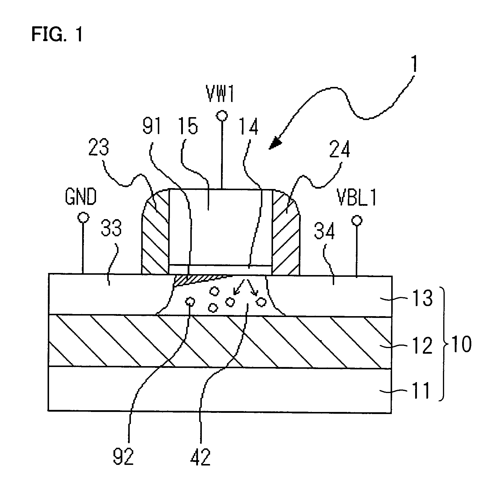
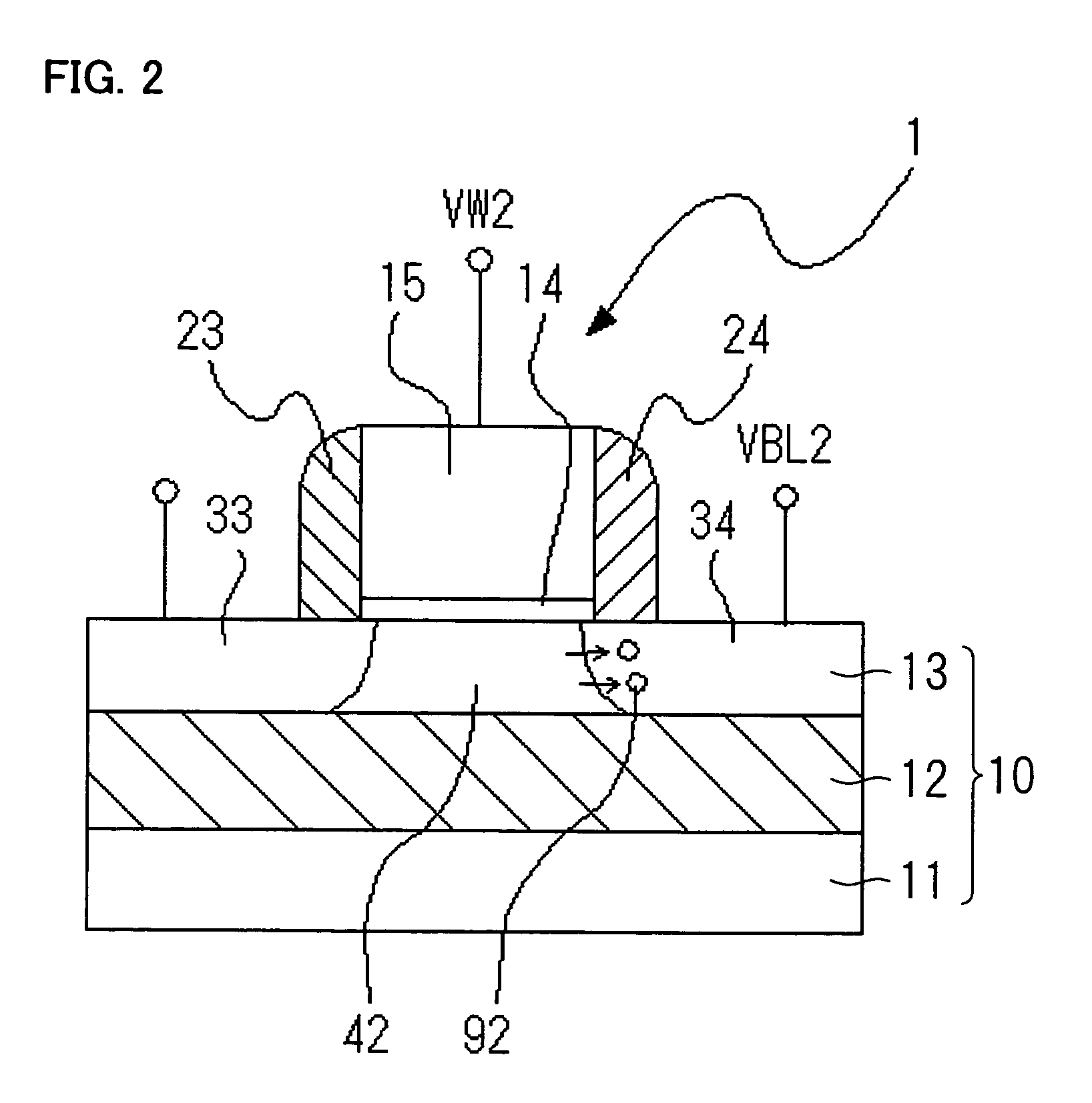
[0050]The volatile memory element (semiconductor device, semiconductor storage device) of the present embodiment is constituted of a single transistor so as to have a function similar to a DRAM, and requires refreshment at constant intervals.

[0051]As shown in FIG. 1, a volatile memory element (first field effect transistor) 1 includes mainly a well region or body region 42, a gate insulating film 14, a gate electrode 15 formed on the gate insulating film 14, diffusion layers (source / drain region, first and second diffusion layer regions) 33 and 34 formed on both sides (both sides of the well region or body region 42) of the gate electrode 15, and a channel region (not shown) disposed under the gate electrode 15.

[0052]The volatile memory element 1 functions as a memory element which can store at least binary information in accordance with an amount of electric charge stored in the well region or body region.

[0053]The volatile memory element 1 is provided on a semiconductor substrate ...

embodiment 2

[0078]Each of FIG. 3 and FIG. 4 shows a structure of the nonvolatile memory element (semiconductor device, semiconductor storage device) of the embodiment of the present invention. As shown in FIG. 3, the nonvolatile memory element (second field effect transistor) 3 is constituted mainly of diffusion layer regions (third and fourth diffusion layer regions) 35 and 36, a body region 43, memory function sections 25 and 26, a gate insulating film 14, and a gate electrode 15. Each of the diffusion layer regions 35 and 36 is a first conduction type region (the one of a P-type region and an N-type region). The body region 43 is a second conduction type region (the other of the P-type region and the N-type region) provided between the diffusion layer regions 35 and 36. The memory function sections 25 and 26 are electric charge retaining sections that are provided on the semiconductor substrate 10 so as to respectively cover (i) a borderline between the diffusion layer region 35 and the body...

embodiment 3

[0171]FIG. 7 shows a cross sectional structure of a nonvolatile memory element (semiconductor device, semiconductor storage device) 4 of an embodiment of the present invention. The nonvolatile memory element 4 is formed on a P-type well region 102 formed on a surface of a semiconductor substrate 101. A gate electrode 104 is formed above the P-type well region 102 via a gate insulating film 103. On both sides of the gate electrode 104, memory function sections 105a and 105b are formed.

[0172]Here, the memory function section is a portion of a memory function body or a charge retaining film, and the portion actually stores electric charge. In an example shown in FIG. 7, an upper face and side faces of the gate electrode 104 are sequentially covered by a silicon nitride film 109, having a trap level for retaining electric charge, which functions as the charge retaining film. In the silicon nitride film 109, both side wall sections of the gate electrode 104 function as the memory functio...


PUM


Abstract

A volatile memory element and a nonvolatile memory element, each of which is constituted of a field effect transistor, are formed on a single semiconductor chip. The volatile memory element includes a body region, a gate electrode, and two diffusion layer regions, and varies an amount of a current, flowing between the diffusion layer regions in applying a voltage to a gate electrode, in accordance with an amount of electric charge retained in the body region. The nonvolatile memory element includes diffusion layer regions, a gate electrode, and two memory function sections, and varies an amount of a current, flowing between the diffusion layer regions in applying a voltage to the gate electrode, in accordance with an amount of electric charge retained in the memory function sections. Thus, it is possible to form the volatile memory and the nonvolatile memory on a single chip with a simple process.

Description

[0001]This Nonprovisional application claims priority under 35 U.S.C. § 119(a) on Patent Application No. 2003 / 138686 filed in Japan on May 16, 2003, the entire contents of which are hereby incorporated by reference.FIELD OF THE INVENTION[0002]The present invention relates to a semiconductor device, a semiconductor storage device, a manufacturing method thereof, and a mobile electronic device. More specifically, the present invention relates to a semiconductor storage device and a semiconductor device each of which has a volatile memory and a nonvolatile memory that are provided on a single chip, a manufacturing method of the semiconductor storage device, and a mobile electronic device having either the semiconductor storage device or the semiconductor device.BACKGROUND OF THE INVENTION[0003]Conventionally, there has been developed a process for providing a plurality of elements different from each other in terms of a structure on a single chip, and the process is applied to manufact...

Claims


Application Information

Patent Timeline
Patent Type & Authority Patents(United States)
IPC IPC(8): G11C11/34G11C7/00H01L27/08G11C7/18G11C16/04G11C16/28H01L21/28H01L21/8234H01L21/8242H01L21/8247H01L27/088H01L27/108H01L27/115H01L29/788H01L29/792
CPCG11C7/1012G11C7/18H01L29/7923H01L21/28273G11C16/04G11C2207/002G11C16/28H01L29/40114
Inventor SHIBATA, AKIHIDEIWATA, HIROSHI
Owner SHARP KK
Why Eureka
Try Eureka