

Fused carbon nanotube-nanocrystal heterostructures and methods of making the same
a carbon nanotube and heterostructure technology, applied in the field of nanotechnology, can solve the problems of poor control of the surface coverage and degree of clustering of nanocrystals on nanotubes, high solubility of catalysts, and mixture of tubes, and achieve the effects of precise placement of nanocrystals, enhanced and greater control of the physical properties of nanotubes
- Summary
- Abstract
- Description
- Claims
- Application Information
AI Technical Summary
Benefits of technology
Problems solved by technology
Method used
Image

Examples
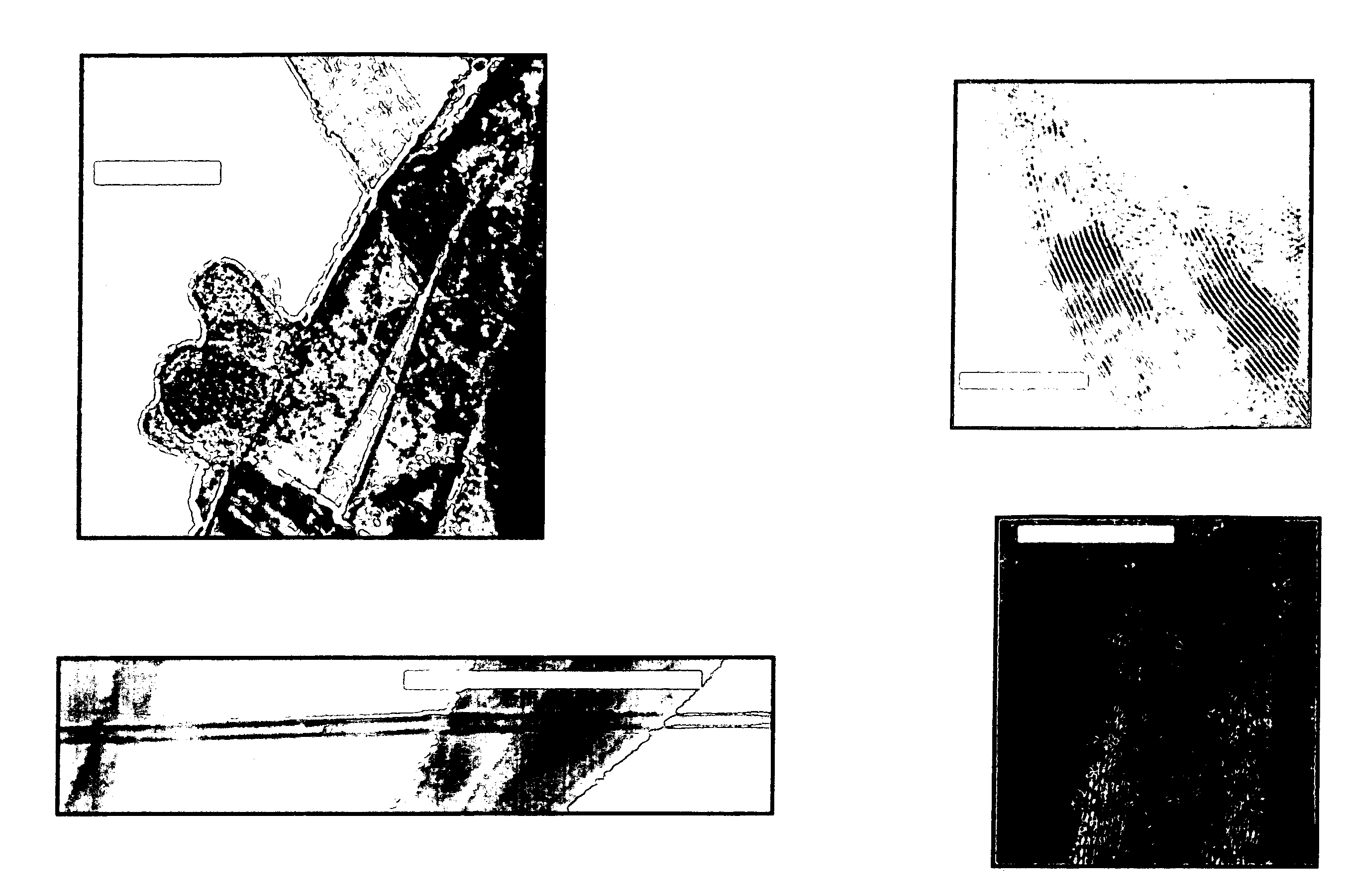
example 1
Synthesis of Multiwalled Nanotube Heterostructures Comprising CdTe Nanocrystals
[0156]Multiwalled nanotubes (MWNTs) were obtained from MER Corporation. An aggressive functionalization protocol was used to remove almost all of the metal impurities (such as iron) and a substantial portion of the amorphous carbon entities in the sample (Hiura et al. Adv. Mater. (Weinheim, Ger.) 7:275 (1995). In essence, a vigorous KMnO4 / H2SO4 treatment was followed by successive processing with solutions of 35% HCl and 10% HF. The purified tubes were then extensively washed with distilled water and heated at 150° C. in a drying oven. XPS analysis, coupled with EDS data, have indicated that any remaining metal was below detectable limits.
[0157]This, rigorous functionalization protocol opens and derivatizes most of the nanotube ends as well as attacks occasional defect sites at the sidewalls (Hirsch, A. Angew. Chem., Int. Ed. 41:1853 (2002) and Banerjee et al. Chem. Eur. J. 9:1898 (2003)). The generated f...
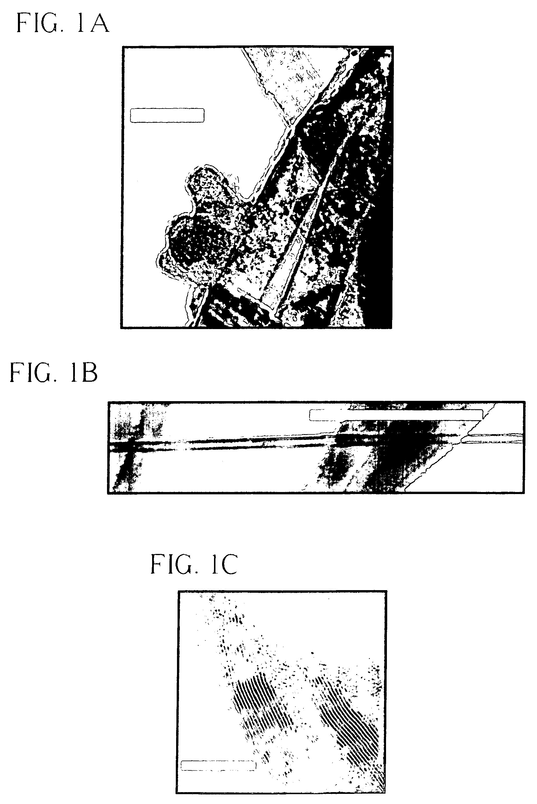
example 2
Synthesis of Single-Walled Nanotube Heterostructures Comprising CdTe Nanocrystals
[0173]Nanotubes were ozonized and oxidized as described in Banerjee et al. J. Phys. Chem B 106:12144 (2002).
[0174]CdO was dissolved in TOPO at 320° C. in the presence of ozonized, oxygenated, and sidewall-functionalized HiPco (high-pressure CO conversion) SWNTs. A substoichiometric amount of tetradecylphosphonic acid (TDPA) was used so that some of the Cd precursor could complex with the tube surface. A solution of tellurium in trioctyl phosphine was rapidly injected at 270° C. and the QDs were allowed to grow at 250° C. under vigorous stirring for 1–20 min. In subsequent workup and purification, toluene was added at 50° C., followed by methanol, which precipitated CdTe nanocrystals in solution. After filtration over a 0.2 μm poly(tetrafluoroethylene) (PTFE) membrane and extensive washing with toluene to remove all unattached nanocrystals, the remaining dark residue was then dried and characterized by l...
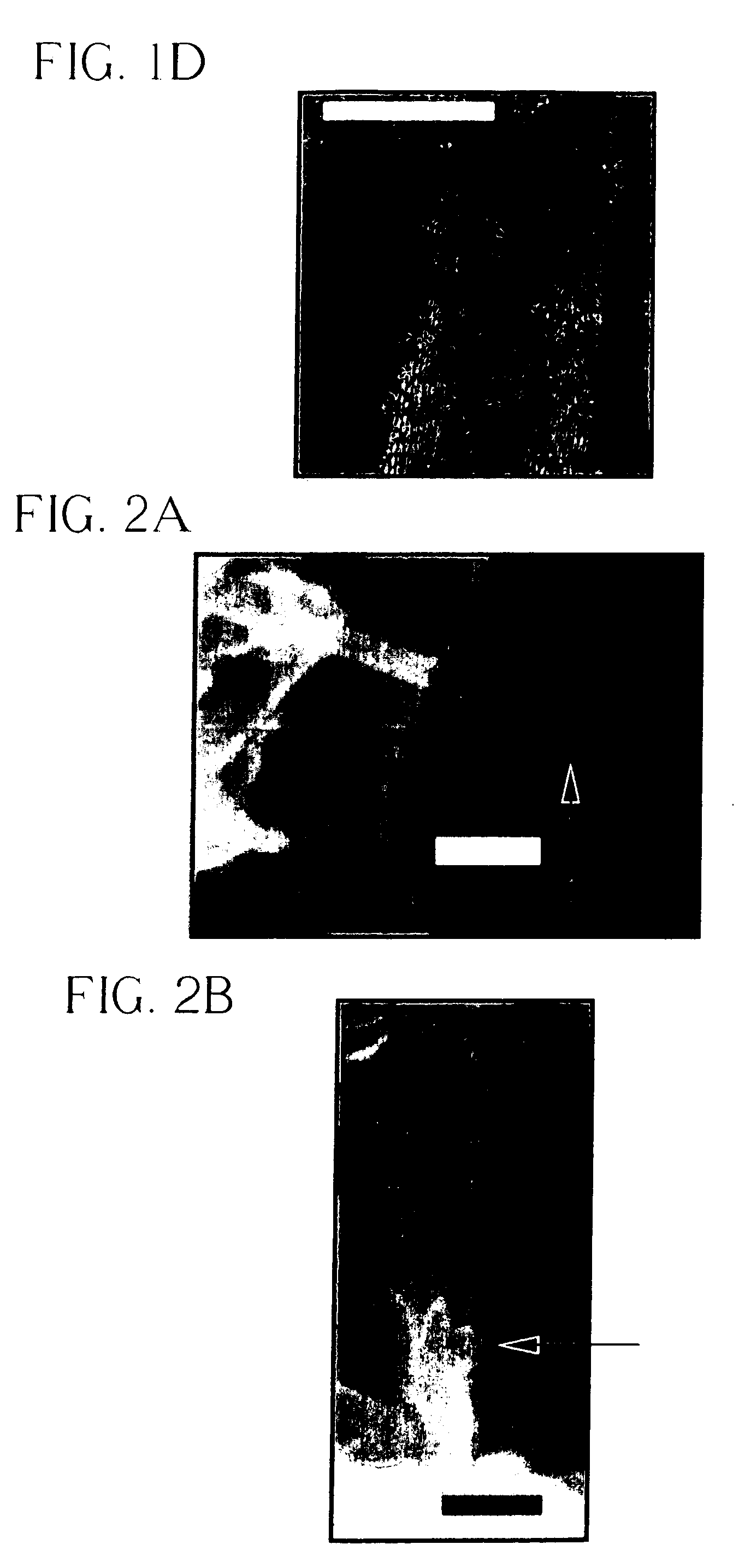
example 3
Synthesis of Single-Walled Nanotube Heterostructures Comprising CdSe Nanocrystals
[0181]Nanotubes were ozonized and oxidized as described in Banerjee et al. J. Phys. Chem B 106:12144 (2002).
[0182]Covalent sidewall functionalization of SWNTs was achieved by an initial treatment with ozone, followed by primary ozonide cleavage with hydrogen peroxide. (See U.S. application Ser. No. 10 / 701,402, incorporated herein by reference.) Carboxylic acids are expected as the predominant functional group on the heavily oxidized nanotube sidewalls. These functional groups, collectively covering up to 30% of the external nanotube surface sites, now act as reactive sites to coordinate onto organometallic metal precursors to CdSe quantum dot formation. Briefly, CdO was dissolved in trioctylphosphine oxide (TOPO) at 320° C., in the presence of ozone / H2O2 treated HiPco (high-pressure CO decomposition) SWNTs. A substoichometric amount of tetradecylphosphonic acid (TDPA) was used to facilitate solubilizati...
PUM
| Property | Measurement | Unit |
|---|---|---|
| diameter | aaaaa | aaaaa |
| diameter | aaaaa | aaaaa |
| diameter | aaaaa | aaaaa |
Abstract
Description
Claims
Application Information