Packaging component and semiconductor package

a technology of packaging components and semiconductors, applied in semiconductor/solid-state device details, semiconductor devices, multi-unit cooking vessels, etc., can solve the problems of deterioration of adhesion between lead frame or another packaging component, deterioration of deterioration of good adhesion between ni-plated layer and sealing resin with time, etc., to achieve excellent heat conduction, excellent electric conduction, and easy work

Active Publication Date: 2007-03-13
SHINKO ELECTRIC IND CO LTD
View PDF15 Cites 24 Cited by
  • Summary
  • Abstract
  • Description
  • Claims
  • Application Information

AI Technical Summary

Benefits of technology

[0059]The packaging component according to the invention comprises a conductor substrate and an electrically conducting layer covering the surfaces thereof. The electrically conducting layer may cover a whole surface of the conductor substrate or may partly cover only the required portions of the surface.
[0060]In the packaging component of the invention, the conductor substrate may be formed from various materials depending upon the constitution of the packaging component or the required characteristics. Suitable materials for forming the conductor substrate may include, for example, copper or an alloy or a compound thereof, as well as an alloy or compound of a metal other than copper (a non-copper metal), though the material of the conductor substrate is in no way limited thereto. Examples of the non-copper metal include aluminum, iron-nickel alloy, etc. When the packaging component is a lead frame, for example, copper or an alloy thereof can be advantageously used as the conductor substrate, because they have excellent electric conduction and can be easily worked. When the packaging component is a heat-radiating plate, it is desired that the conductor substrate exhibits excellent heat conduction and heat radiation. Therefore, copper, aluminum or an alloy thereof can be advantageously used as the conductor substrate.
[0061]The electrically conducting layer may be formed from the same material as the conductor substrate or may be formed from any other materials. The electrically conducting layer is usually formed as a single layer. As required, however, it may be formed as a multi-layer structure having two or more layers. Desirably, the electrically conducting layer is formed as a plated layer by using a plating method. As required, however, it may be formed by a thin-film forming technology other than the plating method, such as vacuum evaporation or sputtering.
[0062]In the case of the packaging component of the invention, the electrically conducting layer covering the conductor substrate must at

Problems solved by technology

Here, there arises a serious problem of deterioration of adhesion between the lead frame or another packaging component (e.g., heat-radiating plate) in the semiconductor package and the sealing resin.
However, as the Ni-plated layer has a low shearing strength at the interface, good adhesion cannot be maintained between the Ni-plated layer and the sealing resin.
The adhesion between the Ni-plated layer and the sealing resin tends to deteriorate with time.
As a result, the sealing resin can expand developing defects such as cracks and causing the semiconductor elements to be peeled.
As a result, cracks occur in the interface between the lead frame or the semiconductor element and the sealing resin, and the sealing resin peels o

Method used


Image

  • Packaging component and semiconductor package
  • Packaging component and semiconductor package
  • Packaging component and semiconductor package

Examples


example 1

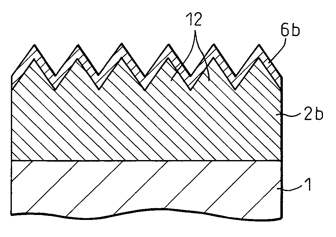
Formation of a Rough-Surface Ni-Plated Layer:

[0119]A copper alloy (trade name: CDA194) containing a trace amount of iron (Fe) was used as a starting material, and the surface on one side thereof was electroplated with nickel to form rough-surface Ni-plated layers at different thicknesses, thereby preparing the following four samples.

[0120]

Sample A:layer thickness of 0.5 μmSample B:layer thickness of 1.0 μmSample C:layer thickness of 3.0 μmSample D:layer thickness of 5.0 μm

[0121]The composition of the electroplating bath and the plating conditions used in this example were as follows: Nickel chloride plating bath:

[0122]

Nickel chloride75 g / LSodium thiocyanate15 g / LAmmonium chloride30 g / LpH:about 4.5 to 5.5Bath temperature:normal temperature (about 25° C.)Cathode current density:about 1 to 3 A / cm2

[0123]The samples A to D having lusterless surface each was:[0124](A) Observed for their surface states by using a scanning electron microscope (SEM, ×10,000),[0125](B) Observed for their cros...

example 2

Formation of a Smooth-Surface Ni-Plated Layer:

[0132]A copper alloy (trade name: CDA194) containing a trace amount of iron (Fe) was used as a starting material, and the surface on one side thereof was electroplated with nickel to form smooth-surface Ni-plated layers at different thicknesses, thereby preparing the following four samples.

[0133]Sample I: layer thickness of 0.5 μm

[0134]Sample II: layer thickness of 1.0 μm

[0135]Sample III: layer thickness of 3.0 μm

[0136]Sample IV: layer thickness of 5.0 μm

[0137]The composition of the electroplating bath and the plating conditions used in this example were as follows: Nickel sulfamate plating bath:

[0138]

Nickel sulfamate320 g / LBoric acid 30 g / LNickel bromide 10 g / LpH:about 3.0 to 4.0Bath temperature:about 30 to 50° C.Cathode current density:about 3 to 30 A / cm2

[0139]The samples I to IV having matte surface each was:[0140](A) Observed for their surface states by using a scanning electron microscope (SEM, ×10,000),[0141](B) Observed for their ...

example 3

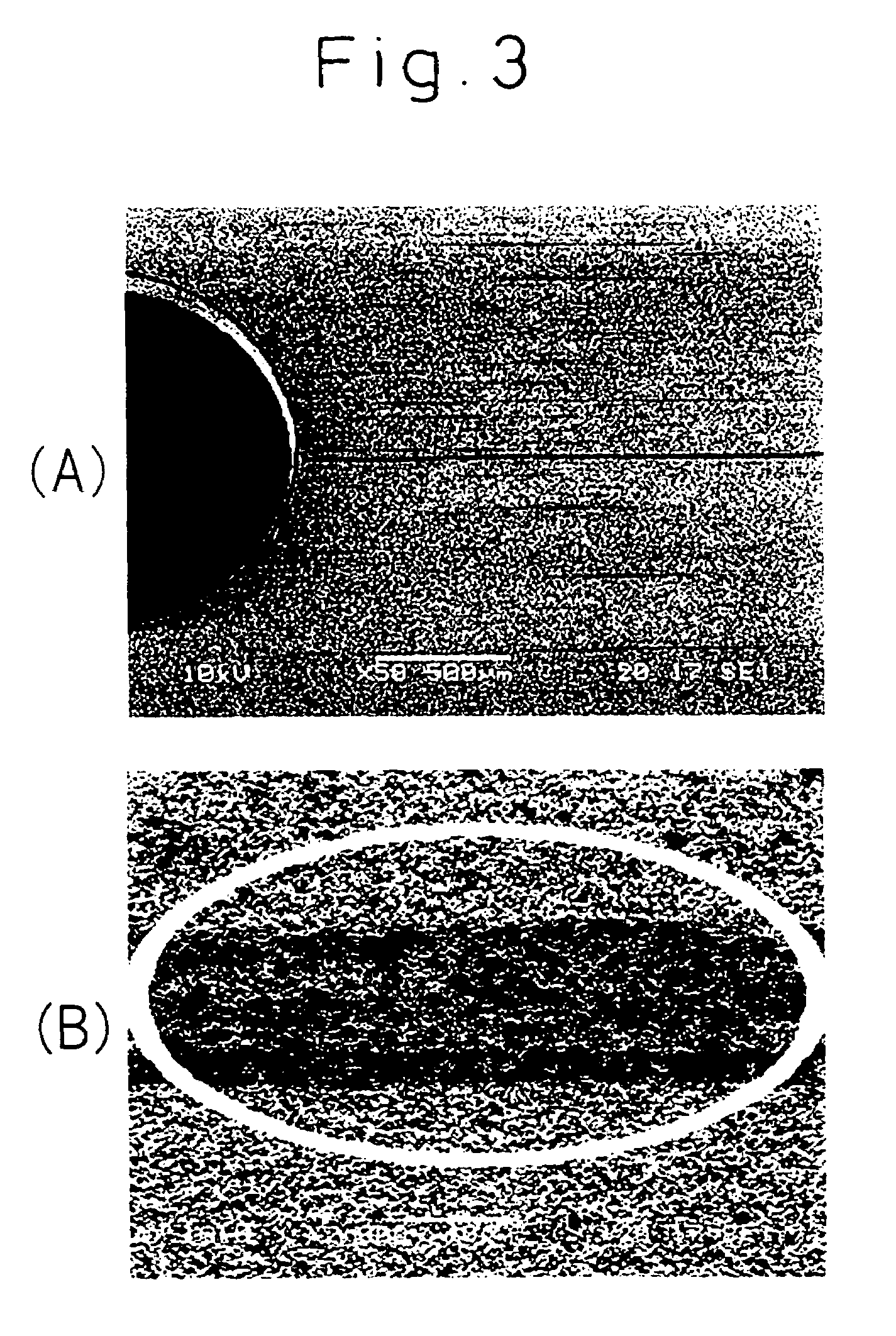
Measurement of the Cup Shear Strength:

[0153]In this example, the samples A to D prepared in Example 1 and the samples I to IV prepared in Example 2 were measured for their cup shear strengths according to the procedure specified under SEMI Standard G69-0996 to evaluate the adhesion of the resin to the rough-surface Ni-plated layer and to the smooth-surface Ni-plated layer.

[0154]First, cups 21 in the shape of a circular truncated cone having a height h of 3 mm, a bottom diameter d1 of 3.568 mm, an upper diameter d2 of 3 mm and a surface area of 10.2 mm2 as illustrated in FIG. 26A were molded by using the following two types of sealing resins:

[0155]Sealing resin A—OCN type (produced by “N” Company)

[0156]Sealing resin B—BNL type (produced by “H” Company)

[0157]The cup 21 was placed on a sample (lead frame) 1 as illustrated in FIG. 26(B) and was heated (post-cured) at 175° C. for 6 hours.

[0158]After the cup 21 was cured and formed upon heating on the sample 1, a gauge (not shown) was pus...


PUM

PropertyMeasurementUnit
Thicknessaaaaaaaaaa
Electrical conductivityaaaaaaaaaa
Structureaaaaaaaaaa

Abstract

A packaging component used for constituting a package mounting a semiconductor element, and a semiconductor package using the packaging component. The packaging component has on at least a portion of the surface thereof a covered surface which is sealed with an insulating resin or on which an adhesive layer is applied, and the packaging component comprises a conductor substrate and an electrically conducting layer partly or entirely covering the surface thereof, and the electrically conducting layer comprises a rough-surface plated layer having a roughened surface profile on the covered surface. The packaging component includes, for example, a lead frame and a heat-radiating or heat-dissipating plate.

Description

BACKGROUND OF THE INVENTION[0001]1. Field of the Invention[0002]The present invention relates to a packaging component and, more particularly, to a part and other elements for use in packaging. The packaging component is useful for the formation of packages having a structure obtained by mounting a semiconductor element or other elements on the packaging component and sealing the element-mounting portion with an insulating resin, and packages in which an adhesive layer is used as a bonding means. The packaging component includes, for example, a lead frame and a heat-radiating or -dissipating plate used in the production of an electronic device. The invention is further relates to a semiconductor package equipped with the packaging component of the present invention and other packages.[0003]2. Description of Related Art[0004]As is well known, there have been proposed a variety of semiconductor packages mounting a semiconductor element such as an IC chip or an LSI chip on a substrate ...

Claims


Application Information

Patent Timeline
IPC IPC(8): H01L23/02C25D5/02H01L23/50C25D5/12C25D7/12H01L23/433H01L23/495
CPCC25D5/02C25D5/12C25D7/12H01L23/49582H01L24/48H01L2924/15747H01L2924/01084H01L2924/01024H01L2924/01023H01L2924/3025H01L2924/16152H01L2924/15311H01L2924/14H01L2924/014H01L23/4334H01L24/45H01L2224/16H01L2224/45144H01L2224/48091H01L2224/48247H01L2224/484H01L2224/48599H01L2224/73204H01L2224/73253H01L2224/85439H01L2224/85464H01L2924/01002H01L2924/01004H01L2924/01005H01L2924/01006H01L2924/01011H01L2924/01013H01L2924/01015H01L2924/01028H01L2924/01029H01L2924/01033H01L2924/01046H01L2924/01047H01L2924/0105H01L2924/01078H01L2924/01079H01L2924/01082H01L2924/01088H01L2924/00014H01L2924/00H01L2224/48639H01L2224/48664H01L2924/12042H01L2924/181H01L2924/18301C25D5/627C25D5/617C25D5/605C25D5/611H01L2924/00012H01L2224/0401A47J27/13H05B6/6408
Inventor SEKI, KAZUMITSUYOSHIE, TAKASHISATO, HARUNOBUMIYAHARA, YOSHIHITO
Owner SHINKO ELECTRIC IND CO LTD
Why Eureka
Try Eureka