Method of wafer/substrate bonding

a technology of substrate and bonding, which is applied in the direction of basic electric elements, electric devices, solid-state devices, etc., can solve the problem of virtually impossible to remove all hydrogen content, and achieve the effects of high bonding strength, good bonding quality, and convenient application

Inactive Publication Date: 2007-03-20
AGENCY FOR SCI TECH & RES
View PDF33 Cites 26 Cited by
  • Summary
  • Abstract
  • Description
  • Claims
  • Application Information

AI Technical Summary

Benefits of technology

[0017]An advantage of the described embodiment of the invention is that the components can be bonded at a relatively low temperature between 300° C. and 200° C. or less, and at the same time ensuring good bonding quality such as high bonding strength and bubble-free interfaces.
[0018]A further advantage of the described embodiment of the invention is that each individual process step is simple and easy to apply and compatible with the existing bonding techniques so that the proposed method can be carried out at a low cost.

Problems solved by technology

It should be noted that it is virtually impossible to remove all hydrogen content since hydrogen may be introduced due to contamination, for example during the deposition process.

Method used


Image

  • Method of wafer/substrate bonding
  • Method of wafer/substrate bonding
  • Method of wafer/substrate bonding

Examples


Embodiment Construction

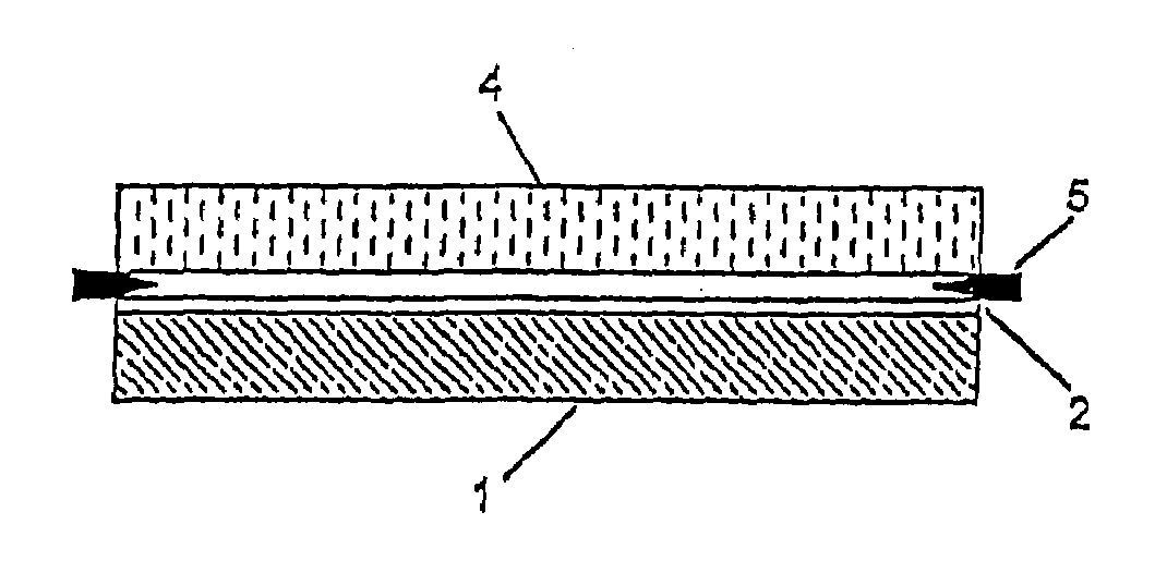
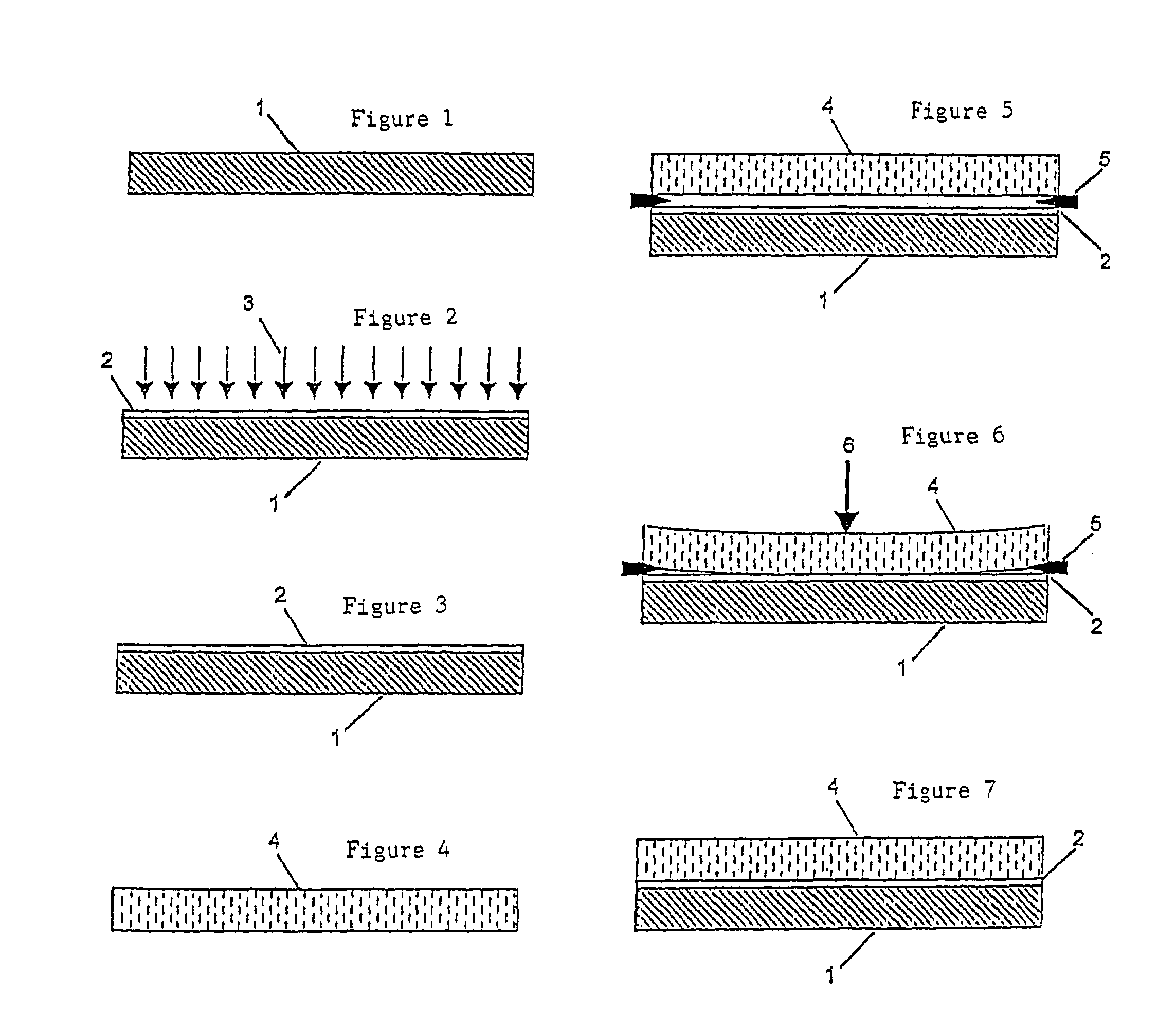
[0040]FIG. 1 illustrates a first component in the form of a wafer 1 to be bonded for example, a semiconductor, ceramic, glass, or other materials, whereas FIG. 4 illustrates a second component in the form of a glass wafer 4. A suitable type of glass material is borosilicate glass or other types of glass material having alkaline ions may be used. In this embodiment, Pyrex 7740 glass is used as the glass wafer 4 for the bonding operation.

[0041]In this embodiment, silicon will be used as an example for the first wafer 1. The conditioning of the silicon wafer 1 may take the form of polishing the surface for the bonding operation so that the surface is a “mirror-polished surface”, which has a surface roughness of typically in the nanometer range. In addition, prior to introduction of the silicon wafer 1 into a deposition chamber, the surface is ultrasonically cleaned by means of a cleansing solvent, for example nitric acid, ammonium hydrogen peroxide, RCA cleansing solution (which can be...


PUM

PropertyMeasurementUnit
temperatureaaaaaaaaaa

Abstract

A method of bonding two components by depositing an amorphous and non-hydrogenated intermediate layer (2) on one of the components (1,4) and arranging the components (1,4) in spaced relationship with the intermediate layer (2) therebetween. The method further comprises heating one or both of the components (1,4) before bringing the components (1,4) into contact. Finally, a voltage is applied to the components (1,4) to create a permanent bond between the two components.

Description

CROSS REFERENCE TO RELATED APPLICATION[0001]This is a U.S. National stage of application No. PCT / SG02 / 00072, filed on 30 Apr. 2002.BACKGROUND AND FIELD OF THE INVENTION[0002]This invention relates to a method of wafer / substrate bonding, particularly but not exclusively, to a method of anodic bonding.[0003]Wafer / substrate bonding has increasingly become a key technology for materials integration in various areas of microelectromechanical systems (MEMS), microoptoelectromechanical systems (MOEMS), microelectronics, optoelectronics and substrate fabrication. It is also widely used for vacuum packaging, hermetic sealing and encapsulation.[0004]In order to bond the wafers / substrates together, various technologies have already been developed, for example, silicon fusion bonding, anodic bonding and intermediate layer bonding, including eutectic, glass frit, solder and adhesive bonding.[0005]Anodic bonding is widely used for bonding between a glass wafer / substrate and a metal or semiconduct...

Claims


Application Information

Patent Timeline
Patent Type & Authority Patents(United States)
IPC IPC(8): H01L21/46H01L21/30H01L21/76C03C27/04C04B37/00C04B37/04H01L21/58
CPCC03C27/042C04B35/64C04B37/00C04B37/04H01L24/26H01L24/83H01L2924/014C04B2235/666C04B2237/52H01L2224/8319H01L2224/8385H01L2924/01018H01L2924/01322H01L2924/07802H01L2924/09701H01L2924/3025H01L2924/01006H01L2924/01023H01L2924/01033H01L2924/3512H01L2924/00H01L2924/12042
Inventor WEI, JUNWANG, ZHIPINGXIE, HONG
Owner AGENCY FOR SCI TECH & RES
Why Eureka
Try Eureka