Reflective substrate and algorithms for 3D biochip

a technology of reflective substrate and biochip, applied in the field of reflective substrate and algorithms for 3d biochip, can solve the problems of complex and unsatisfactory wave dielectric solutions, and achieve the effect of eliminating major background artifact emissions

Active Publication Date: 2007-04-03
BIOCEPT INC
View PDF5 Cites 68 Cited by
  • Summary
  • Abstract
  • Description
  • Claims
  • Application Information

AI Technical Summary

Benefits of technology

[0010]This invention involves the use of a reflective substrate or coating and a transparent dielectric layer in the creation of biochips. The use of such combination has been extensively explored as a means to amplify a signal generated by a fluorophore. However, the current embodiment of the approach eliminates major background artifact emissions within the biochip.
[0011]Pursuant to this teaching, one selects a thickness of a dielectric that yields substantial cancellation at the wavelength of interest generated at its surface. Given a 180 degree phase shift at the reflective (metallic) surface, the thickness may then be an integer multiple of ½ wavelength. For example, if the emission photons are centered at 600 nm (in vacuum), one calculates the corresponding wavelength (600 / refractive index) in the dielectric medium of interest, and then uses a thickness that is some integer multiple of ½ the calculated wavelength. The effect will be to eliminate background that emanates from the top surface of the dielectric i.e. the attachment surface. Cancellation occurs for background emissions that lie within and at the base of the analyte domain, in addition to its neighborhood.

Problems solved by technology

Because a major problem with biochips is the presence of spurious background signal, much of which arises from the plane containing the standard analyte domains, i.e. the plane of attachment, the use of such a %-wave dielectric may not be the entire solution as this background may become amplified with the same gain as the signal from the analyte.
When placed upon a ¼-wave dielectric atop a reflective layer, amplification exists, but it is more complex as different parts of the domain experience constructive or destructive interference, resulting in some cases in distinct ring patterns if the domain is circularly domed.

Method used


Image

  • Reflective substrate and algorithms for 3D biochip
  • Reflective substrate and algorithms for 3D biochip

Examples


example

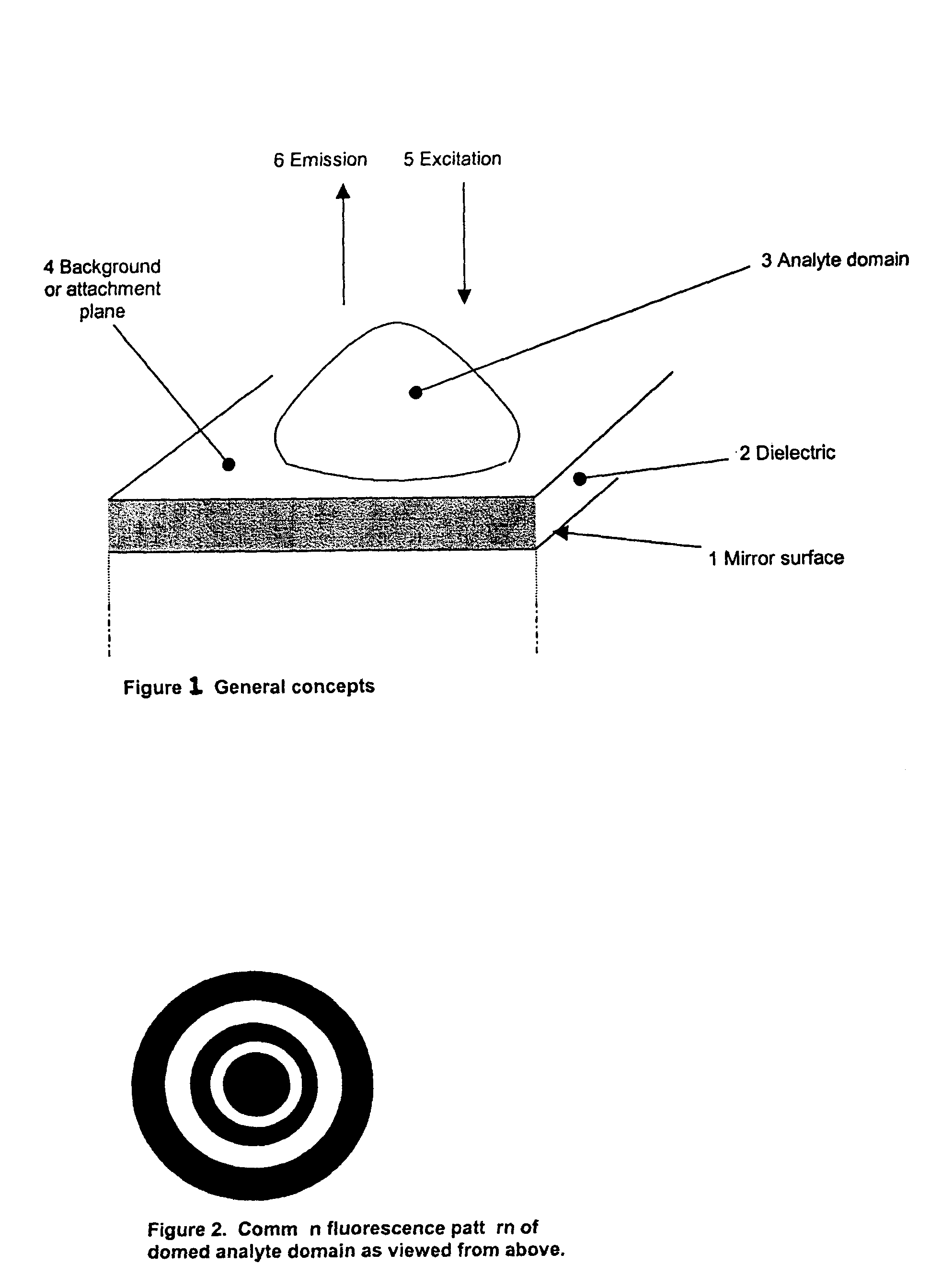
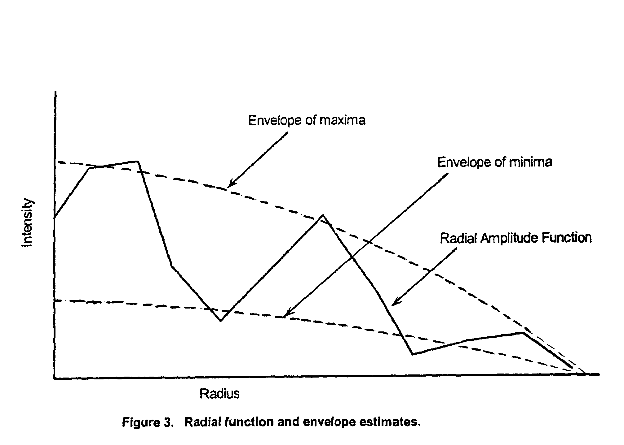
[0044]To test the arrangement, microspots were applied to substrates which contained a mixture of a polyurethane-based hydrogel and Cy5 fluorescent dye so as to form a series of three-dimensional tiny mounds or domains spaced apart on surfaces of the slides. Two different sets were used, the slides of one set were purchased from Corning and were transparent aminosilane-coated slides. The other set of slides were mirrored, having a thin aluminum film that was highly reflective, atop a thin substrate, with the aluminum being coated with a layer of silica of appropriate thickness. These microspots were deposited using two different pin sizes, one set of spots on each set of slides was deposited using large pins having a diameter of about 625 microns and a second set was deposited using small pins having a diameter of 350 microns. Once the microspots had polymerized, both sets of slides were imaged using a Perkin-Elmer ScanArray-Light microarray laser scanner that was set with the appro...


PUM

PropertyMeasurementUnit
refractive indexaaaaaaaaaa
thicknessaaaaaaaaaa
reflectivityaaaaaaaaaa

Abstract

A reflective substrate is used to amplify the photon signal captured from overlying analyte domains containing photon emitters. The reflective substrate provides substantial desired signal amplification of the photon emissions from each domain via interference effects induced in the incident excitation and / or emission energies. A dielectric is interposed between the domains and the reflective surface, which has a thickness such that substantial destructive interference occurs with respect to emission photons or excitation photons or both at the attachment surface. When analyte domains have a three-dimensional structure such that a significant fraction of their volume extends at least ¼ wavelength above the attachment surface provided by the dielectric, substantial constructive signal amplification can take place of signals generated within the analyte domains. Destructive interference relating to emissions arising from the plane of attachment surface yields significant reduction in spurious background emissions.

Description

[0001]This application claims priority from U.S. Provisional Application Ser. No. 60 / 412,522, filed Sep. 19, 2002, the disclosure of which is incorporated herein by reference.BACKGROUND OF THE INVENTION[0002]Biochip is a term used to refer to an array of discrete domains containing biochemical probes that will react with desired targets or analytes. Some means is generally necessary to quantify the amount of bound target, and it is common to employ some form of photon detection. Fluorescence or chemo-luminescence can be employed with spatially resolved fluorescence scanning being by far the most common detection approach. Such a fluorescence imaging system is described in detail in U.S. Pat. No. 5,672,880 (Sep. 30, 1997).[0003]Because of the very small quantities of analyte normally encountered, highly sensitive means are required to detect photon emissions. A large industry has developed around producing scanners used in the detection of signals from biochips.[0004]The present inve...

Claims


Application Information

Patent Timeline
Patent Type & Authority Patents(United States)
IPC IPC(8): C12Q1/68C12M1/36G01N15/06
CPCB01L3/5085G01N21/648B01L2300/0636B01L2300/168
Inventor RACHLIN, DANIEL J.
Owner BIOCEPT INC
Why Eureka
Try Eureka