Pattern defect inspection method and its apparatus

a technology of defect inspection and pattern, applied in the direction of optical radiation measurement, semiconductor/solid-state device testing/measurement, instruments, etc., can solve the problems of pattern damage, pattern shrinkage or expansion, pattern increase to reach the physical limit, etc., and achieve high resolution and high speed

Inactive Publication Date: 2007-04-17
HITACHI HIGH-TECH CORP
View PDF11 Cites 20 Cited by
  • Summary
  • Abstract
  • Description
  • Claims
  • Application Information

AI Technical Summary

Benefits of technology

[0012]The present invention has been made to solve the problems, and an object of the present invention is to provide a pattern defect inspection method, and its apparatus, used to detect a minute circuit pattern with high resolution at high speed by use of ultraviolet light or ultraviolet laser light without causing the damage to a device as a target to be inspected, and thereby to detect a defect.

Problems solved by technology

However, the increase in NA reaches the physical limit.
Thus, when an inspection wavelength extremely gets close to the exposure wavelength, the resist reacts at the time of inspection, causing a pattern to shrink or expand.
Accordingly, there is a possibility that the pattern will be damaged.
Moreover, in a memory part having a narrow line width like a system LSI, or in a chip where a rough wiring part is mixed, irradiating with inspection light causes heat to accumulate in part of the chip.
Therefore, there is also concern that the bimetal effect will cause peeling of a pattern called stress migration.
This means a decrease in mechanical strength, resulting in low adhesion at the time of deposition.
Therefore, there is a possibility that a bad influence will be exerted on a device.
In addition, there is a limit of the heat capacity that is acceptable for the device, which is called thermal budget.
Therefore, it is not possible to use a method in which a thinly narrowed laser beam is scanned on a sample.
On the other hand, if illumination with a laser beam is performed with a visual field being fully opened, a speckle occurs.
Therefore, a high-quality image cannot be obtained.

Method used


Image

  • Pattern defect inspection method and its apparatus
  • Pattern defect inspection method and its apparatus
  • Pattern defect inspection method and its apparatus

Examples


Embodiment Construction

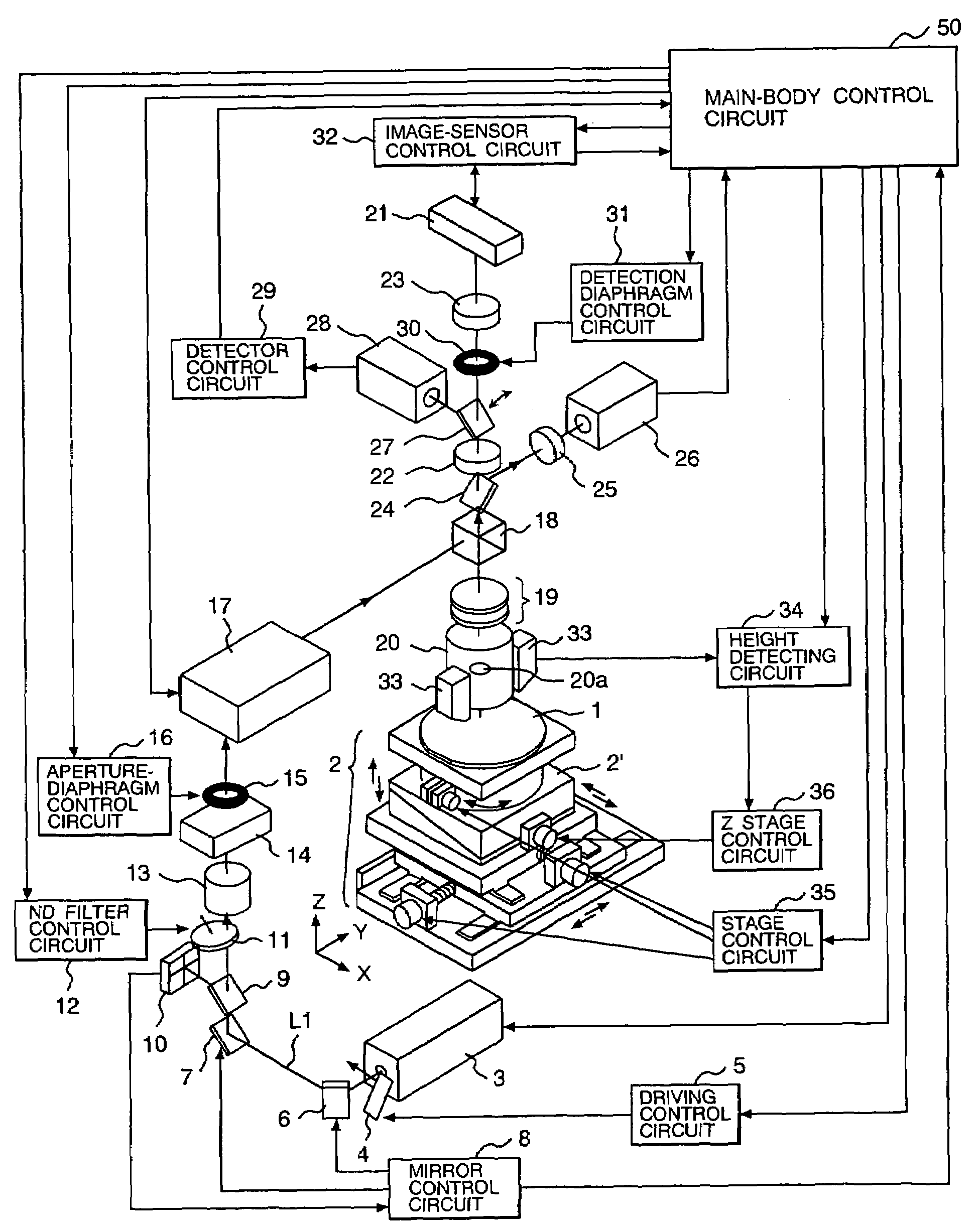
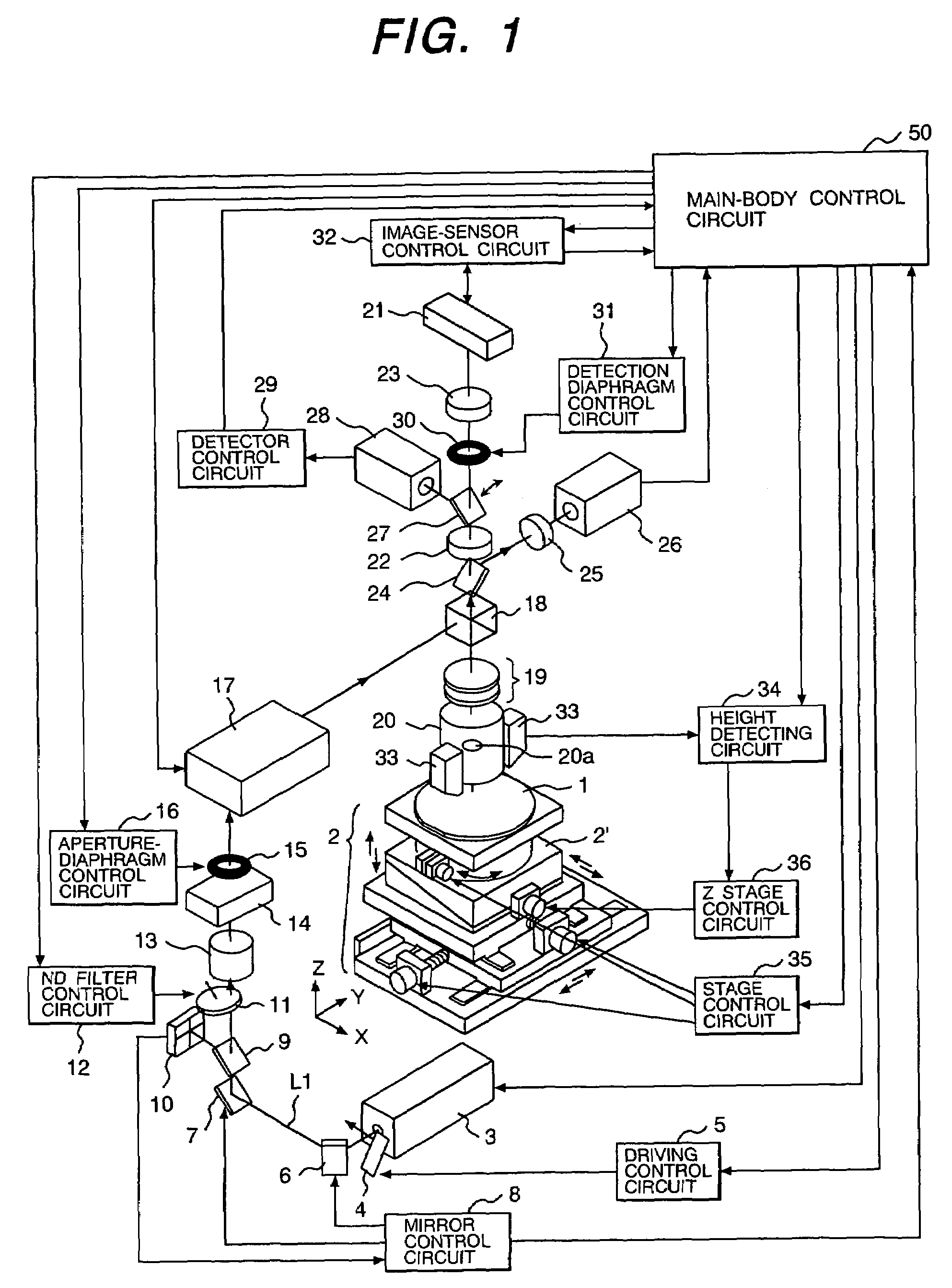
[0055]Embodiments of a defect inspection method for inspecting a pattern to be inspected, and of its apparatus, according to the present invention, will be described with reference to drawings. FIG. 1 is a diagram illustrating one embodiment of the apparatus according to the present invention. A stage 2 is constituted of X, Y, Z, and θ (rotation) stages. A semiconductor wafer (sample) 1 which is an example of a pattern to be inspected is placed on the stage 2.

[0056]An illumination optical system is formed of an irradiation optical system comprising: an illumination light source 3; a shutter 4 that is one of quantity-of-light adjusting unit, and that can switch the quantity of light between a state close to ON and a state close to OFF; mirrors 6, 7 for adjusting optical axis displacement; an ND filter 11 that is one of quantity-of-light adjusting unit; a beam expander 13; an illumination-range formation optical unit 14 for forming a multipoint secondary light source; an aperture diap...


PUM

PropertyMeasurementUnit
sizeaaaaaaaaaa
diameteraaaaaaaaaa
wavelengthaaaaaaaaaa

Abstract

The pattern defect inspection apparatus and its method of the present invention comprises: a recipe setting unit for setting an inspection recipe and/or a review recipe; an illumination optical system including: a laser light source for emitting ultraviolet laser light; a quantity-of-light adjusting unit for adjusting a quantity of the ultraviolet laser light emitted from the laser light source; and an illumination range forming unit for forming on a sample an illumination range of the ultraviolet laser light; a coherence reducing system; and a detection optical system including: a condensing optical system; a diffracted-light control optical system; and a detecting unit.

Description

BACKGROUND OF THE INVENTION[0001]The present invention relates to pattern inspection and foreign material inspection that detect a defect (including a short circuit and a broken wire) and a foreign material of a pattern to be inspected. More particularly, it relates to an inspected-pattern defect inspection method, and its apparatus, used for inspecting a defect and a foreign material on a pattern to be inspected such as a semiconductor wafer, a liquid crystal display, and a photo mask. The description below is based on the assumption that a defect includes a foreign material.[0002]Japanese Patent Laid-open No. 8-320294 (prior art 1) is known as the prior art relating to defect inspection of a pattern to be inspected. This prior art 1 describes the technology comprising the steps of: in a pattern to be inspected such as a semiconductor wafer where an area with high pattern density such as a memory mat unit and an area with low pattern density such as a peripheral circuit are mixed i...

Claims


Application Information

Patent Timeline
Patent Type & Authority Patents(United States)
IPC IPC(8): G01J1/42G01B11/30G01N21/88G01N21/956G06T1/00H01L21/66
CPCG01N21/8806G01N21/956
Inventor YOSHIDA, MINORUMAEDA, SHUNJINISHIYAMA, HIDETOSHIWATANABE, MASAHIRO
Owner HITACHI HIGH-TECH CORP
Why Eureka
Try Eureka