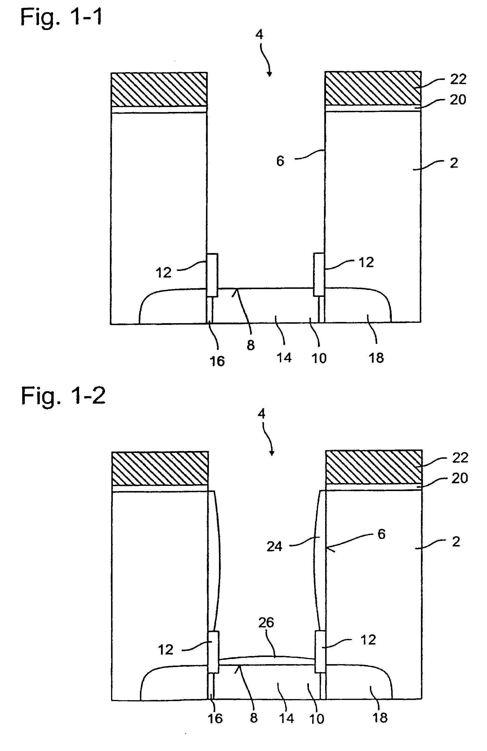
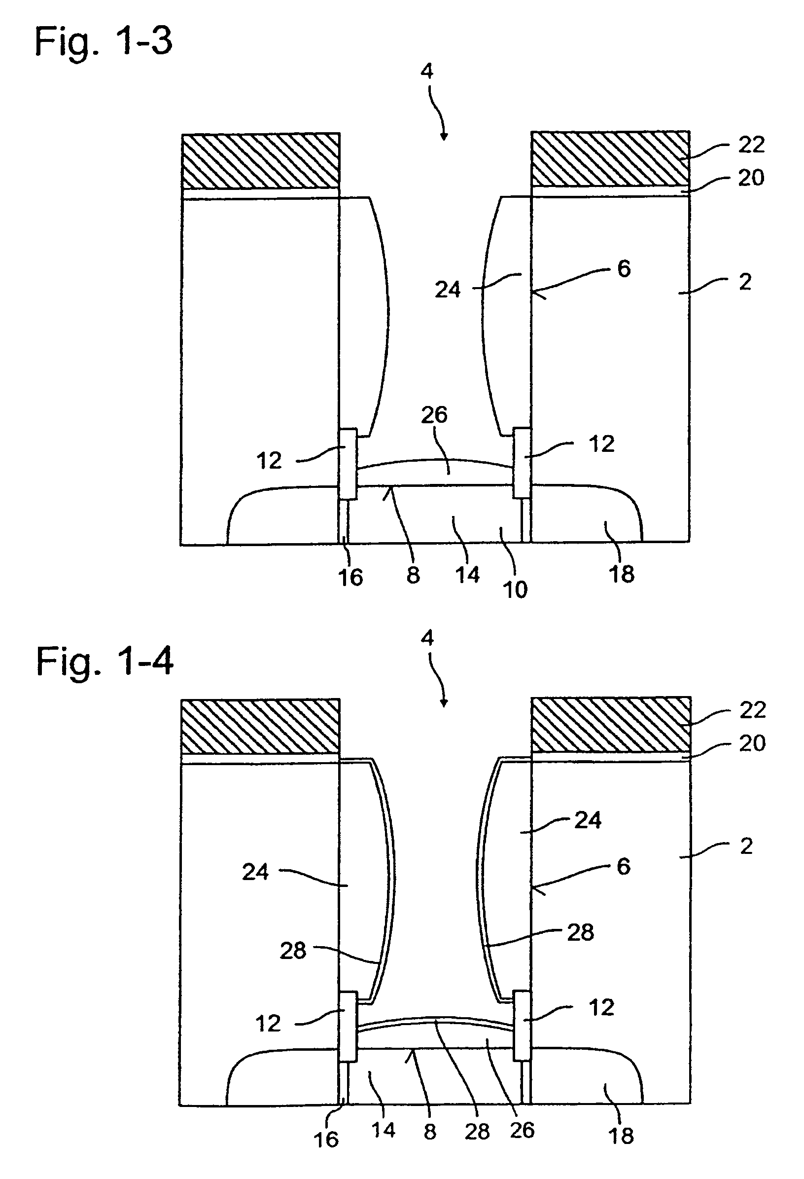
[0019]According to the present invention, the epitaxial semiconductor layer neither fills the entire trench, as in U.S. Pat. No. 6,093,614, nor grows together with the polysilicon which has been deposited on the base of the trench, as in U.S. Pat. No. 5,365,097, but rather the semiconductor layers are deposited with a space being left between them. This advantageously prevents the formation of an epitaxial closing joint and of crystal
lattice defects. In particular, the epitaxial semiconductor layer which grows onto the side wall is free of defects, so that a perfect
transistor channel can form at that location. In order also to suppress the formation of crystal lattice defects during subsequent steps, in which the space is filled with a conductive material, a thin dielectric, which only partially limits an
electric current, is formed at least on the epitaxial semiconductor layer. This fulfills two functions. Firstly, the epitaxial semiconductor layer which has grown on the side wall is isolated from semiconductor layers which are not in
single crystal form, so that crystal lattice defects cannot spread to the epitaxial semiconductor layer. The thin dielectric therefore fulfills the function of a matching or buffer layer between the deposited conductive material and the epitaxial semiconductor layer. Secondly, the thin dielectric limits the
diffusion of dopants out of the conductive material into the epitaxial semiconductor layer and into the adjacent single-crystal semiconductor substrate. The
doping region which is formed in the process is therefore more compact and does not extend as far into the single-crystal semiconductor substrate. The risk of
doping regions of adjacent transistors overlapping one another is considerably reduced. Therefore, the trenches in which the vertical transistors are formed can also be arranged spatially closer together. A further
advantage of the vertical transistor which has been fabricated in this way includes the freedom of choice with regard to the setting of the channel cross section and the channel length. The channel length is substantially predetermined by the length of the epitaxial layer. By contrast, the cross section of the channel is predetermined by the thickness of this layer.
[0020]The deposition of the semiconductor layers preferably takes place selectively with respect to the material of the transition region, so that the semiconductor layers grow on the substrate of semiconductor material. The selectivity also leads to semiconductor layers of better quality.
[0024]Since the
crystallinity of the deposited semiconductor layers is dependent, inter alia, on the
crystallinity of the substrates on which they have been deposited, the semiconductor layer which has been deposited at the base of the trench grows in polycrystalline form. Furthermore, it is expedient if the epitaxial semiconductor layer is doped in situ while it is being formed. The extent of the doping can be changed during the deposition. If the cross section of the trench is assumed to be circular or elliptical, it is possible to produce regions of identical or different
dopant concentration, running in the shape of a circle or concentrically, in order to optimally set the properties of the
transistor channel. A broad channel cross section with a homogeneous characteristic, if appropriate with an increased
dopant concentration toward the
gate dielectric, is advantageous.
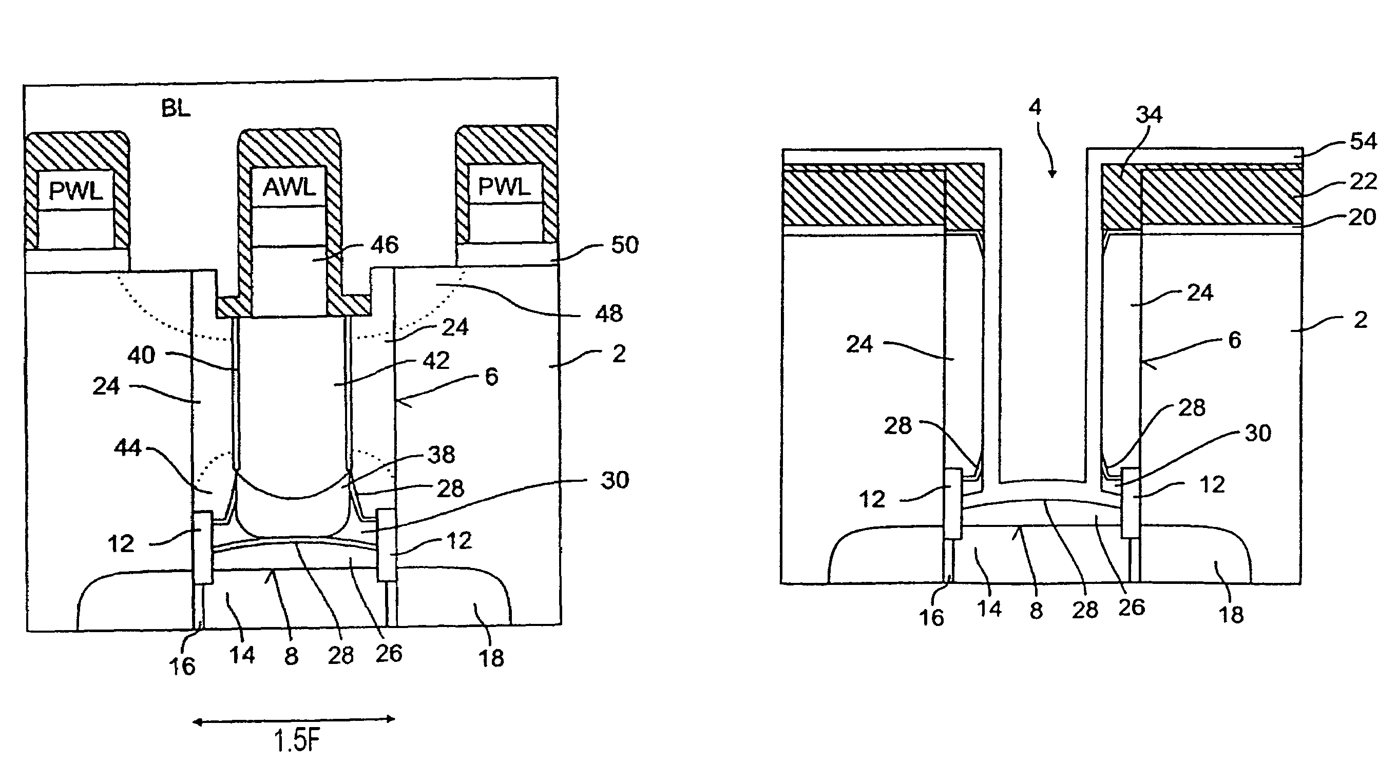
[0042]It has proven to be a particular
advantage that the trench can have a cross section whose extent is greater than the minimum feature size which can be achieved by
lithography and is used, for example, for the fabrication of lateral transistors. Compared to a laterally formed transistor, a vertical transistor does not require any additional lateral space. Therefore, the individual
capacitor trenches can be arranged closer together. The minimum lateral distance between two
capacitor trenches (measured from the trench wall of one
capacitor trench to the trench wall of the adjacent capacitor trench), however, is determined by the size of the outdiffusion regions (buried straps) which are formed to make contact between the inner capacitor electrodes and the drain regions of the select transistors. In this context, the invention makes it possible to reduce this distance further, since the extent of the outdiffusion regions is limited on account of the thin dielectric and these regions do not extend as far into the semiconductor substrate. The outdiffusion region may preferably also be formed behind a protective cladding, in order to limit the outdiffusion region substantially to the epitaxial semiconductor layer. By way of example, the insulation collar of the trench capacitor represents a protective cladding of this type. The reduction in the minimum lateral distance which is made possible by the method according to the invention on the other hand makes it possible to increase the size of the cross section of the trenches while retaining a constant packing density of the capacitor trenches. The increase in the
diameter leads to a range of process technology advantages for the fabrication of the trench capacitor. In particular, all the
etching, patterning and deposition steps in the capacitor trench can be carried out more easily on account of the increased space available. Examples of these steps are the
etching of the capacitor trench itself, the formation of the insulation collar in the upper part of the capacitor trench, the formation of the storage dielectric and the deposition of the filler material in order to form the inner capacitor
electrode. Furthermore, the larger cross section of the capacitor trench also leads to a reduced series resistance of the inner capacitor
electrode. It is also easier to carry out measures which increase the surface area in the capacitor trench in order to increase the storage
capacitance; in this context, hemispherical
silicon grains (HSG) or wavy trenches could be mentioned.

