Method of manufacturing piezoelectric thin film device and piezoelectric thin film device

a piezoelectric thin film and piezoelectric technology, applied in piezoelectric/electrostrictive devices, piezoelectric/electrostrictive/magnetostrictive devices, piezoelectric/electrostriction/magnetostriction machines, etc., can solve the problem of affecting the etching rate affecting the yield of piezoelectric thin film devices on substrates, and affecting the etching rate o

Active Publication Date: 2007-05-01
MEMS SOLUTIONS INC
View PDF14 Cites 38 Cited by
  • Summary
  • Abstract
  • Description
  • Claims
  • Application Information

AI Technical Summary

Benefits of technology

[0018]The present invention is made in view of the above-mentioned problems, and an object of the present invention is to provide a method of producing a piezoelectric thin film device having excellent characteristics and high reliability, which is capable of forming a space for oscillation excellently under a piezoelectric laminated structure with a simple process, and a piezoelectric thin film device produced by this method.
[0032]As described above, by combining the insulating layer capable of being etched by the specific chemical substance and the sacrificial layer having a higher etching rate than the insulating layer by the specific chemical substance, the space for oscillation can be formed excellently under the piezoelectric laminated structure by a simple process without using a polishing technology such as a CMP, etc., and the piezoelectric thin film device having excellent characteristics and high reliability can be produced stably. Further, since the piezoelectric thin film device of the present invention has an excellent space for oscillation under the piezoelectric laminated structure, the characteristics are excellent and the reliability is high. Therefore, it is suitable to produce a piezoelectric thin film device such as a filter, a duplexer, etc., by combining the piezoelectric laminated structure having the obtained oscillation space.

Problems solved by technology

This disturbs the integration of the piezoelectric thin film resonators.
Therefore, an insertion loss of the piezoelectric thin film device produced by combining a plurality of the piezoelectric thin film resonators becomes remarkably large.
A large via hole of an opening size of 930 μm is not only easy to be damaged, but also an acquired quantity of the final product, that is, a yield of the piezoelectric thin film device on the substrate is limited, and a region of about 1 / 15 of the substrate can be used for a device production.
However, the via hole is further increased in size, a strength of the device is remarkably reduced, and the resonators are further easy to be damaged.
However, this method requires long and complicated steps.
Since the manufacturing steps are long and complicated, the method itself increases the cost of the device as well as reduces a yield of the product, and further the device becomes highly costly.
When the piezoelectric laminated structure is formed on this sacrificial layer, a decrease in an electromechanical coupling factor Kt2 associated with a decrease in a crystal orientation of the piezoelectric thin film itself, and a decrease in a resonant sharpness Q associated with an increase in a surface roughness of the piezoelectric laminated structure itself, occur, and production of the piezoelectric thin film device having good characteristics becomes difficult.
Thus, there is a problem in stability of the polymer.
Further, since a bend of 2000 nm arises at ends of the piezoelectric laminated structure, there is a severe problem of remarkable deterioration of reliability by cracking or a decrease in strength of the piezoelectric thin film.
Accordingly, it is necessary to form the device with use of a material durable to two types of etchants, which restricts the material to be used and which makes the process complex, thereby increasing the production cost.
When these substances form a film by a vapor-depositing method, etc., the surface roughness of the sacrificial layer is large, and crystal orientation of the lower electrode and the piezoelectric thin film formed on the sacrificial layer is deteriorated.
Further, when the bend of the piezoelectric thin film is large, the strength of the piezoelectric thin film decreases, and reliability remarkably decreases.
Therefore, it becomes remarkably difficult to stably obtain the piezoelectric thin film device having excellent characteristics and high reliability.
By such a reason, a piezoelectric thin film device which performs sufficient performance in gigahertz band has not been obtained.

Method used


Image

  • Method of manufacturing piezoelectric thin film device and piezoelectric thin film device
  • Method of manufacturing piezoelectric thin film device and piezoelectric thin film device
  • Method of manufacturing piezoelectric thin film device and piezoelectric thin film device

Examples


example 1

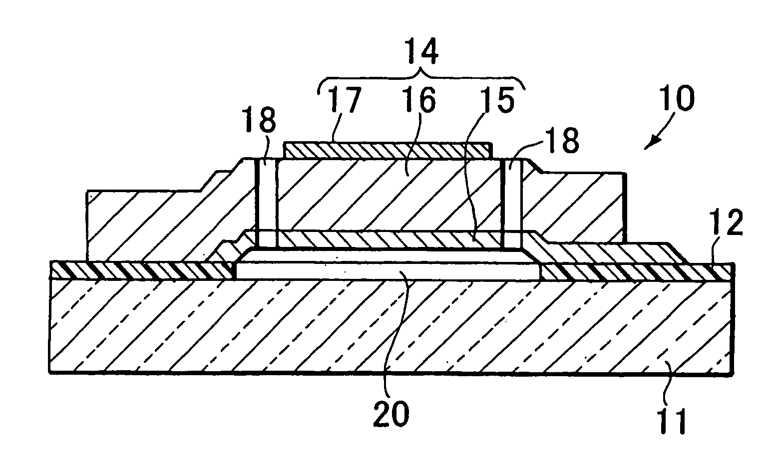
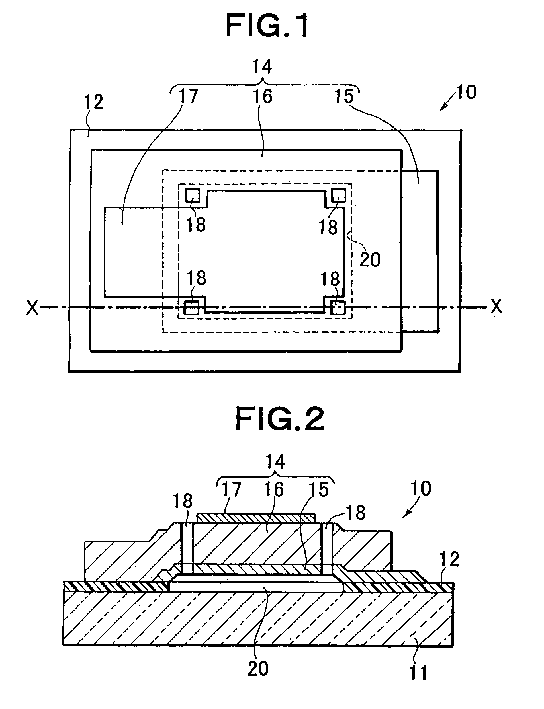
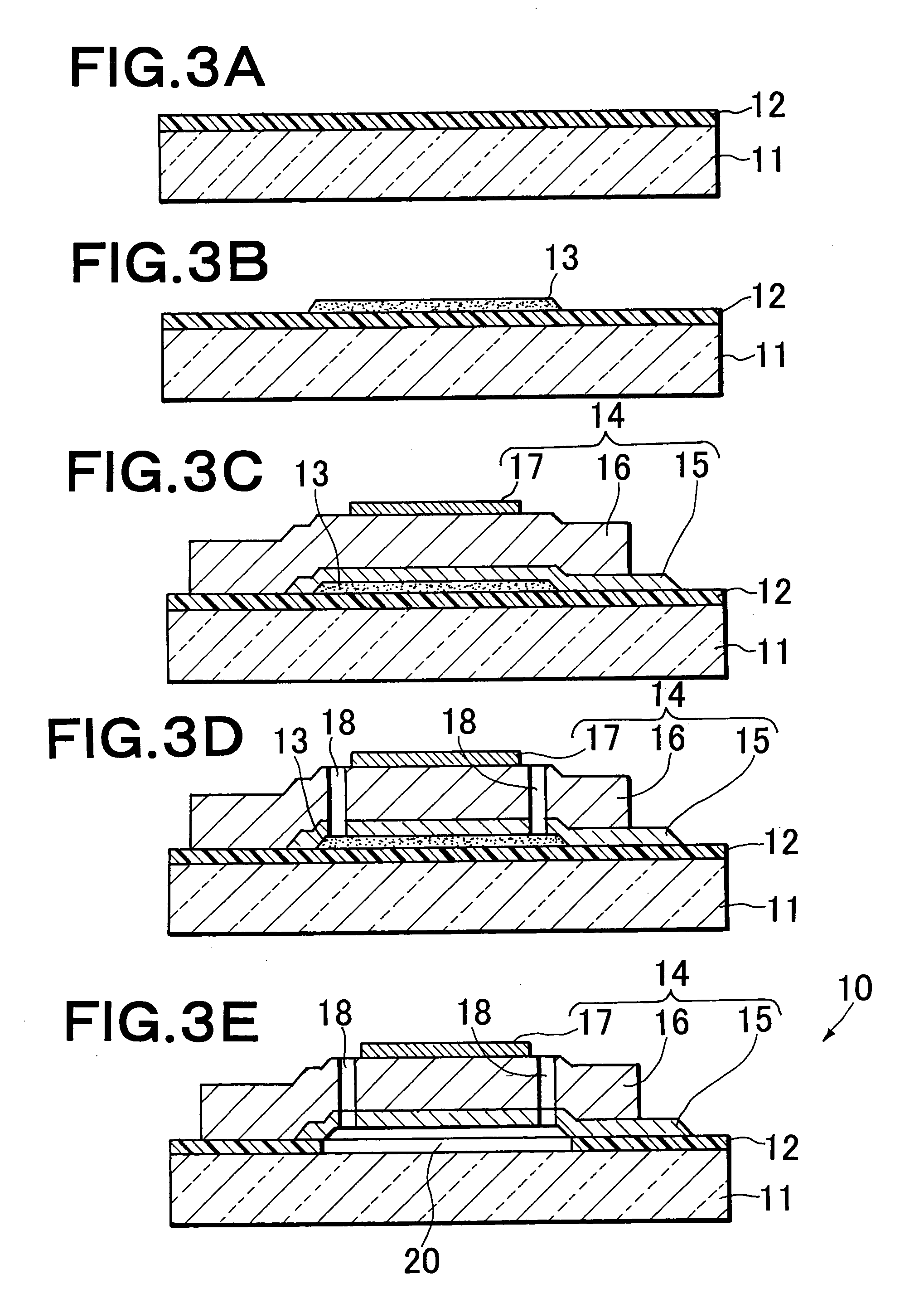
[0066]In this example, a piezoelectric thin film device (piezoelectric thin film resonator) constituted as shown in FIGS. 1 and 2 was produced as below.

[0067]That is, an SiO2 layer having a thickness of 2000 nm was formed by a thermal oxidation method as an insulating layer, on both surfaces of a 6-inch Si wafer having a thickness of 625 μm. The upper surface of the Si wafer was coated with a photoresist, and a lift-off pattern for a sacrificial layer for forming a space for oscillation shown in FIG. 1 was formed. After a Ti layer of 50 nm was formed as a sacrificial layer on an upper surface side of this Si wafer by a DC magnetron sputtering method under the conditions of gas pressure of 0.5 Pa without heating a substrate, an ultrasonic wave was applied thereto in a resist removing liquid to pattern the sacrificial layer in a desired shape. Then, the upper surface of this Si wafer was coated with the photoresist. A lift-off pattern for a lower electrode as shown in FIG. 1 was forme...

example 2

[0071]In this example, as described below, the piezoelectric thin film device (piezoelectric thin film resonator) constructed as shown in FIGS. 1 and 2 was produced. That is, except that the thickness of the insulating layer was 1000 nm, the piezoelectric thin film resonator shown in FIGS. 1 and 2 was produced by a method similar to the method shown in Example 1.

[0072]The forming method of the insulating layer, the material and thickness of the insulating layer, the material and thickness of the sacrificial layer, and the electromechanical coupling factor Kt2, resonant sharpness Q and the defective fraction of the obtained piezoelectric thin film resonator in this example were as shown in Table 1, wherein Kt2=6.2%, Q=1300 and the defective fraction was 0.4%.

example 3

[0073]In this example, as described below, the piezoelectric thin film device (piezoelectric thin film resonator) constructed as shown in FIGS. 1 and 2 was produced. That is, except that the forming method of the insulating layer was CVD method and the thickness of the insulating layer was 3000 nm, the piezoelectric thin film resonator shown in FIGS. 1 and 2 was produced by a method similar to the method shown in Example 1.

[0074]The forming method of the insulating layer, the material and thickness of the insulating layer, the material and thickness of the sacrificial layer, and the electromechanical coupling factor Kt2, resonant sharpness Q and the defective fraction of the obtained piezoelectric thin film resonator in this example were as shown in Table 1, wherein Kt2=6.5%, Q=1070 and the defective fraction was 0.3%.


PUM

PropertyMeasurementUnit
thicknessaaaaaaaaaa
thicknessaaaaaaaaaa
surface roughnessaaaaaaaaaa

Abstract

Method of producing a piezoelectric thin film device comprises a step of forming an insulating layer (12) capable of being etched by a specific chemical substance on the upper surface of a substrate (11); a step of forming a sacrificial layer (13) made of a substance having a higher etching rate by the specific chemical substance than the insulating layer on a partial region of the insulating layer; a step of forming a lower electrode (15) on a region including the sacrificial layer; a step of forming the piezoelectric thin film (16) on a region including a part of the lower electrode; a step of forming an upper electrode (17) on a region including a part of the piezoelectric thin film; a step of forming via hole (18), which penetrates the piezoelectric thin film and lower electrode, so as to expose a part of the sacrificial layer; and a step of forming a space (20) for oscillation by etching both the sacrificial layer and the insulating layer with the same specific chemical substance by introducing the specific chemical substance through the via hole.

Description

[0001]This application is a 371 of PCT / JP2004 / 018890 filed on Dec. 17, 2004 and claims priority benefits from Japanese Patent Application Number 2003-422211 filed Dec. 19, 2003.TECHNICAL FIELD[0002]The present invention relates to a method of producing a piezoelectric thin film device produced by combining single or a plurality of piezoelectric thin film resonators using a piezoelectric thin film, and more particularly to a method of producing piezoelectric thin film device used for a filter for communication equipment, or the like, and a piezoelectric thin film device produced by the same.BACKGROUND ART[0003]Devices using a piezoelectric phenomenon have been used in various fields. In the progress of miniaturization and power saving of portable equipment, the application field of surface acoustic wave (SAW) devices as RF filters or IF filters used for the above equipment is being enlarged. Enhancement of the design and producing technologies of SAW filters have satisfied user's str...

Claims


Application Information

Patent Timeline
Patent Type & Authority Patents(United States)
IPC IPC(8): H03H9/15H03H3/02H03H9/54H01L41/09H01L41/187H01L41/22H03H3/04H03H9/17
CPCH01L41/316H03H3/04H03H9/173H03H9/174H10N30/076
Inventor NAGAO, KEIGOKUNISAWA, TETSUROYAMADA, TETSUO
Owner MEMS SOLUTIONS INC
Why Eureka
Try Eureka