
Optical transmission substrate, method for manufacturing optical transmission substrate and optoelectronic integrated circuit

a technology of optical transmission substrate and optical transmission substrate, which is applied in the direction of circuit optical details, optical elements, instruments, etc., can solve the problems of difficult to realize the performance of even interconnection within the board, the rate control of the computer performance, and the difficulty of high-performance mounting boards

Active Publication Date: 2007-05-01
INT BUSINESS MASCH CORP
View PDF14 Cites 31 Cited by
  • Summary
  • Abstract
  • Description
  • Claims
  • Application Information

AI Technical Summary

Problems solved by technology

The technological innovations over the years are reaching a territory where computer performance is subjected to rate-controlling depending on how fast data transfer to / from other elements is performed and not on improvement in a switching speed of a semiconductor element or an operating clock.
Along with the above requirement, it has been more and more difficult to realize sufficient performance of even interconnect within the board by use of electric interconnect.
However, a high-performance mounting board, in which the electric interconnect and the optical interconnect are mixed by use of a possible method as an industrialization process, has not yet been realized.
When the optical waveguide is provided on the surface of the mounting substrate, the optical waveguide is damaged in mounting electronic components or optical components and a difference in thermal expansion coefficient between the mounting substrate and an optical waveguide material causes the mounting substrate to bend.
In the method of patent documents 1 and 2, it takes time to sequentially install the optical fibers and it is difficult to mechanize a method for forming an input / output portion of light to the optical fibers.
Thus, the method is not suitable for mass production.
In addition, the input / output portion of the optical fiber is mechanically weak and easily damaged.
Moreover, it takes effort to exchange the optical fibers when damaged.
Furthermore, it is impossible to perform wiring by use of, for example, a radius of curvature (for example, about 20 mm or less) which is smaller than the least curvature of the optical fiber.
Consequently, application to a high-density optical / electric mounting board is difficult.
In addition, large-sized vacuum equipment is required in the conventional manufacturing method.
Thus, this method is not suitable as a method for forming an optical waveguide in a large mounting board.
Moreover, there is a problem that it is difficult to thicken the optical waveguide structure by sputtering or the like in order to form a 50×50 μm square multimode optical waveguide which is easily subjected to optical coupling.
Thus, it is difficult to couple light of the optical waveguide to the optical element through a thick mounting substrate.
Thus, there is a problem that it is highly likely that the optical waveguide and the optical element are damaged by mechanical, thermal and chemical processing in a laminate process, a built-up process and the like for an electronic circuit, which should be performed after formation of the optical waveguide.
Furthermore, in the method of patent document 4, in the case of performing a process of forming the optical waveguide after mounting an electronic device, there is a possibility that the electronic devices are damaged.
Meanwhile, in the case of mounting the electronic device after forming the optical waveguide, there is a possibility that the optical waveguide exposed to a lower surface of the mounting substrate is damaged.
Thus, there is a possibility that the optical waveguide is damaged by warp in the mounting substrate caused by temperature rise in the middle of a manufacturing process of the mounting substrate, temperature rise within a case in operation of the electronic device and the like.
Thus, compared to the case of connecting the both cores directly to each other, light is diffused and coupling loss occurs.
Thus, the coupling loss is increased.
Thus, there is a possibility that an optical output portion is damaged by chips including chips of electrodes or the like.
Thus, it is difficult to align a cross-section portion of a tip of an optical guide pin with a height of a core portion of the optical waveguide.
Thus, the coupling loss is increased.
As described above, in the method for aligning the cross-section portion of the tip of the optical guide pin with the height of the core portion of the optical waveguide by making the through-hole and inserting the optical guide pin into the through-hole thereabove, the alignment is difficult and the coupling loss occurs.
Thus, it is difficult to realize a high-performance optical / electric mounting substrate.
Moreover, in the method of nonpatent document 3, it is difficult to realize a sufficient coupling efficiency in the case where light is focused in a thickness direction of a thick mounting substrate by use of a lens relay system and the light is received by a photodetector.
Thus, light focusing by use of the lens relay system becomes extremely difficult.
Moreover, in the method of nonpatent document 4, in the formation of an optical / electric mounting substrate by mounting a polymer optical waveguide on an electronic circuit, the exposed optical waveguide is damaged in mounting electronic components.
Moreover, deterioration and warp are caused by heat.
Thus, it is difficult to realize a high-performance mounting substrate.

Method used


Image

  • Optical transmission substrate, method for manufacturing optical transmission substrate and optoelectronic integrated circuit
  • Optical transmission substrate, method for manufacturing optical transmission substrate and optoelectronic integrated circuit
  • Optical transmission substrate, method for manufacturing optical transmission substrate and optoelectronic integrated circuit

Examples


Embodiment Construction

[0056]The present invention will be described below through embodiments of the invention. However, the invention according to scope of claims is not limited to the following embodiments. Moreover, not all combinations of features described in the embodiments are essential to solving means of the invention.

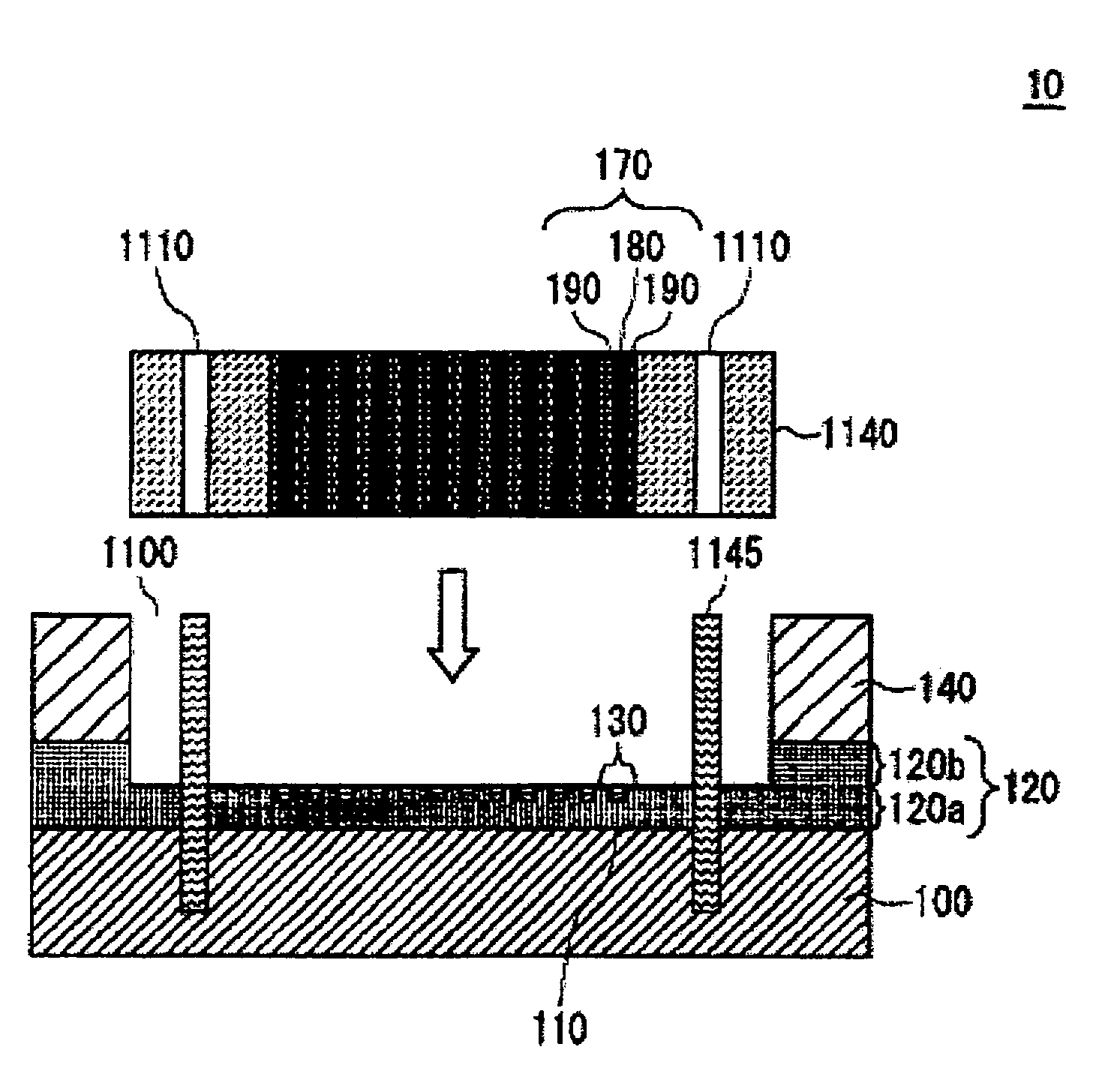
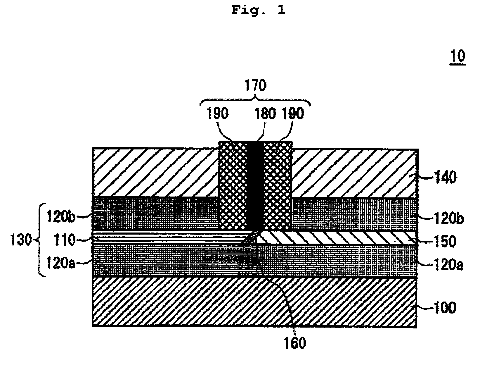
[0057]FIG. 1 shows a configuration of an optical transmission substrate 10 according to this embodiment. The optical transmission substrate 10 according to this embodiment has the configuration in which an optical waveguide 130 is provided between a first substrate 100 and a second substrate 140 and light reflected from the optical waveguide 130 toward the second substrate 140 is guided to vicinity of an upper surface of the second substrate 140 by an optical fiber 170. Thus, positioning of an end of the optical waveguide 130 and the optical fiber 170 is facilitated and a high coupling efficiency can be realized. Moreover, the provision of the optical waveguide 130 between the firs...


PUM


Abstract

Provided is an optical transmission substrate including: a first substrate; an optical waveguide which has clad covering a core and a periphery of the core and extends on an upper surface of the first substrate; a second substrate provided parallel to the first substrate so that a lower surface thereof contacts an upper surface of the optical waveguide; a reflection surface which is provided on a cross section of the core at an end of the optical waveguide and reflects light, which travels through the core of the optical waveguide, toward the second substrate; and a light guide which is provided in the second substrate and guides the light, which is reflected toward the second substrate, toward an upper surface of the second substrate from a position closer to the core than an upper surface of the clad.

Description

BACKGROUND OF THE INVENTION[0001]The present invention relates to an optical transmission substrate, a method for manufacturing an optical transmission substrate and an optoelectronic integrated circuit. Particularly, the present invention relates to an optical transmission substrate including an optical waveguide therein, a method for manufacturing an optical transmission substrate and an optoelectronic integrated circuit.[0002]The technological innovations over the years are reaching a territory where computer performance is subjected to rate-controlling depending on how fast data transfer to / from other elements is performed and not on improvement in a switching speed of a semiconductor element or an operating clock. Thus, connection within a board or between boards by use of a terabit-class ultra-high speed, large-capacity interconnect has been required. Along with the above requirement, it has been more and more difficult to realize sufficient performance of even interconnect wi...

Claims


Application Information

Patent Timeline
Patent Type & Authority Patents(United States)
IPC IPC(8): G02B6/26G02B6/12G02B6/36G02B6/38G02B6/42G02B6/122G02B6/125G02B6/13G02B6/30G02B6/43H05K1/02
CPCG02B6/125G02B6/30G02B6/4214G02B6/43G02B2006/12104H05K1/0274H05K1/144
Inventor FUKUZAWA, TADASHIHASEGAWA, MASAKI
Owner INT BUSINESS MASCH CORP
Learn More