Integrated circuit having a low power, gain-enhanced, low noise amplifying circuit

a low-power, gain-enhanced, low-noise technology, applied in the direction of dc-amplifiers with dc-coupled stages, amplifiers with semiconductor devices/discharge tubes, different amplifiers, etc., can solve the problems of increased power consumption, increased die size, and increased noise, etc., to achieve low power and low noise

Active Publication Date: 2007-05-08
CHIPCON +1
View PDF5 Cites 33 Cited by
  • Summary
  • Abstract
  • Description
  • Claims
  • Application Information

AI Technical Summary

Problems solved by technology

A fundamental challenge in the design of a low noise amplifier (LNA) in an integrated circuit (IC) with a relatively small current consumption is to achieve a sufficient transconductance of the active devices for determining its gain and noise performance.
The trade-offs between the signal gain, the noise figure, and the bias current are especially difficult with Complementary Metal-Oxide Semiconductor (CMOS) LNAs due to the inherent low transconductance of Metal-Oxide Semiconductor Field Effect Transistors (MOSFETs).
This approach, however, is not the most cost-effective due to the silicon area penalty or increased bill-of-material.
The performance advantages of differential RF circuits are, in most cases, a trade-off with the resulting increase in power consumption and larger die size.
This circuit has some drawbacks, such as high input and output impedances which require external matching networks in order to match to well-accepted impedance levels (e.g. 50 ohms).
Finally, the design is inherently a single-ended circuit topology which is not always optimal from the standpoint of noise immunity in highly integrated designs.
One common drawback of these circuits is the large number of inductors required for impedance matching and signal transfer purposes.
The use of such inductors results in either a prohibitively large silicon area for IC design or a large number of external components.

Method used


Image

  • Integrated circuit having a low power, gain-enhanced, low noise amplifying circuit
  • Integrated circuit having a low power, gain-enhanced, low noise amplifying circuit
  • Integrated circuit having a low power, gain-enhanced, low noise amplifying circuit

Examples


first embodiment

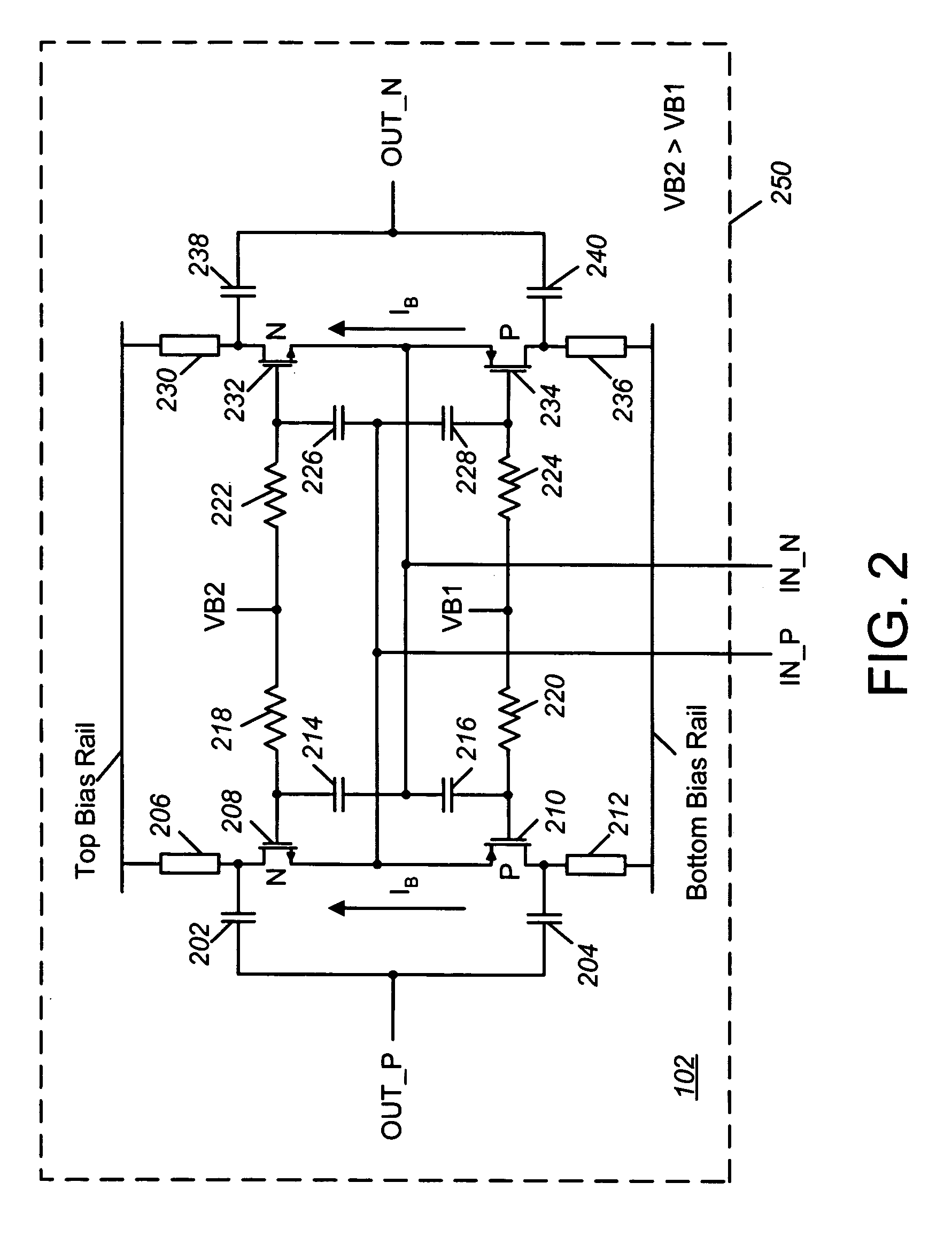
[0019]Referring now to FIG. 2, a schematic diagram of a low power, gain-enhanced, low noise amplifying (LNA) circuit 102 of the present application is shown. In FIG. 2, amplifying circuit 102 is a full differential amplifier (i.e. both the input signal and the output signal are fully differential) which may be used as LNA 102 of FIG. 1. Amplifying circuit 102 is preferably embodied in an integrated circuit (IC) 250.

[0020]A differential input signal is presented at the differential input of LNA 102 which is represented by IN_N and IN_P nodes. The differential input (i.e. the IN_N and IN_P nodes) is provided at and exposed externally on IC 250 in the form of conductive pads or leads. As shown in FIG. 2, the IN_N node is coupled to first ends of capacitors 214 and 216, a source of a negative-channel (n-channel) transistor 232, and a source of a positive-channel (p-channel) transistor 234. Preferably, n-channel transistor 232 is an N-channel Metal Oxide Semiconductor Field Effect Transi...

second embodiment

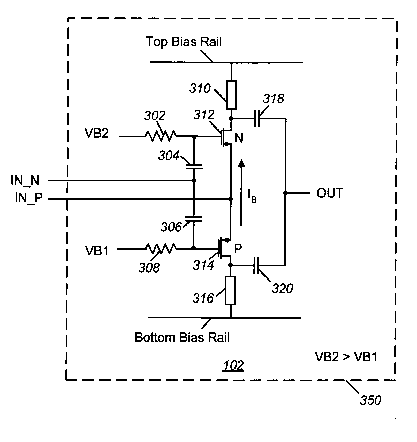
[0027]FIG. 3 is amplifying circuit 102 of the present application which is embodied within an IC 350. Amplifying circuit 102 of FIG. 3 provides an input which is adapted to receive a differential signal, but an output that is single-ended. Otherwise, the amplifying circuit of FIG. 3 is similarly structured and functions as a half portion of the amplifying circuit of FIG. 2.

[0028]Amplifying circuit 102 of FIG. 3 includes an n-channel transistor 312, a p-channel transistor 314, capacitors 304, 306, 318, and 320, impedance circuits 310 and 316, and resistors 302 and 308 (optional). A differential input is represented by and at IN_N and IN_P nodes, whereas a single-ended output is represented by and at an OUT node. The IN_N node is provided at first ends of capacitors 304 and 306, which have second ends coupled to the gates of transistors 312 and 314, respectively. The IN_P node is provided at sources of transistors 312 and 314. A drain of n-channel transistor 312 is coupled to a first ...


PUM


Abstract

An amplifying circuit includes an n-type transistor having a source, a gate coupled to a first bias voltage, and a drain coupled to a first supply voltage through a first impedance circuit. A p-type transistor of the circuit has a source coupled to the source of the n-type transistor, a gate coupled to a second bias voltage, and a drain coupled to a second supply voltage through a second impedance circuit. A first differential input is coupled to the gate of the n-type transistor through a first capacitor and to the gate of the p-type transistor through a second capacitor. A second differential input is coupled to the sources of the n-type and the p-type transistors. A third capacitor has a first end coupled to the drain of the n-type transistor, and a fourth capacitor has a first end coupled to the drain of the p-type transistor and a second end coupled to a second end of the third capacitor. An output of the amplifier circuit is provided at the second ends of the third and the fourth capacitors. The n-type transistor and the first impedance circuit serve as a common-source amplifier for a signal at the first differential input and as a common-gate amplifier for the signal at the second differential input. Similarly, the p-type transistor and the second impedance circuit serve as a common-source amplifier for the signal at the first differential input and as a common-gate amplifier for the signal at the second differential input.

Description

BACKGROUND[0001]1. Field of the Technology[0002]The present application relates generally to the fields of electronic circuits, microelectronics, and radio frequency (RF) integrated circuit (IC) design, and more particularly to a low noise amplifier (LNA) which provides high signal gain with low power consumption by sharing a bias current among active devices of the LNA.[0003]2. Description of the Related Art[0004]A fundamental challenge in the design of a low noise amplifier (LNA) in an integrated circuit (IC) with a relatively small current consumption is to achieve a sufficient transconductance of the active devices for determining its gain and noise performance. The trade-offs between the signal gain, the noise figure, and the bias current are especially difficult with Complementary Metal-Oxide Semiconductor (CMOS) LNAs due to the inherent low transconductance of Metal-Oxide Semiconductor Field Effect Transistors (MOSFETs). For a constant current draw, the performance of high fr...

Claims


Application Information

Patent Timeline
Patent Type & Authority Patents(United States)
IPC IPC(8): H03F3/26
CPCH03F3/193H03F3/45264
Inventor ROINE, PER TORSTEIN
Owner CHIPCON
Why Eureka
Try Eureka