Post passivation interconnection schemes on top of the IC chips

a technology of interconnection schemes and ic chips, applied in the direction of semiconductor devices, semiconductor/solid-state device details, electrical devices, etc., can solve the problems of fissures and cracks, and the inability of two approaches to create thick metal, and achieve high resistivity of interconnection lines

Inactive Publication Date: 2007-06-12
QUALCOMM INC
View PDF13 Cites 67 Cited by
  • Summary
  • Abstract
  • Description
  • Claims
  • Application Information

AI Technical Summary

Benefits of technology

[0027]It is therefore of interest to the semiconductor art to provide a method of creating interconnect lines that removes typical limitations that are imposed on the interconnect wires, such as unwanted parasitic capacitances and high interconnect line resistivity. The present invention is related to U.S. Pat. No. 6,303,423, to the same assignee as the present invention.
[0028]A principal objective of the invention is to provide a method for the creation of interconnect metal that allows for the use of thick and wide metal.

Problems solved by technology

This is because an inorganic material cannot be deposited as a thick layer of dielectric because such a layer of dielectric could develop fissures and crack as a result.
Either one of these two approaches cannot create thick metal due to cost considerations or oxide crackingthick, wide interconnect lines can be created by first sputtering a thin metal base layer, coating and patterning a thick layer of photoresist, applying a thick layer of metal by electroplating, removing the patterned photoresist and performing metal base etching (of the sputtered thin metal base).

Method used


Image

  • Post passivation interconnection schemes on top of the IC chips
  • Post passivation interconnection schemes on top of the IC chips
  • Post passivation interconnection schemes on top of the IC chips

Examples


Embodiment Construction

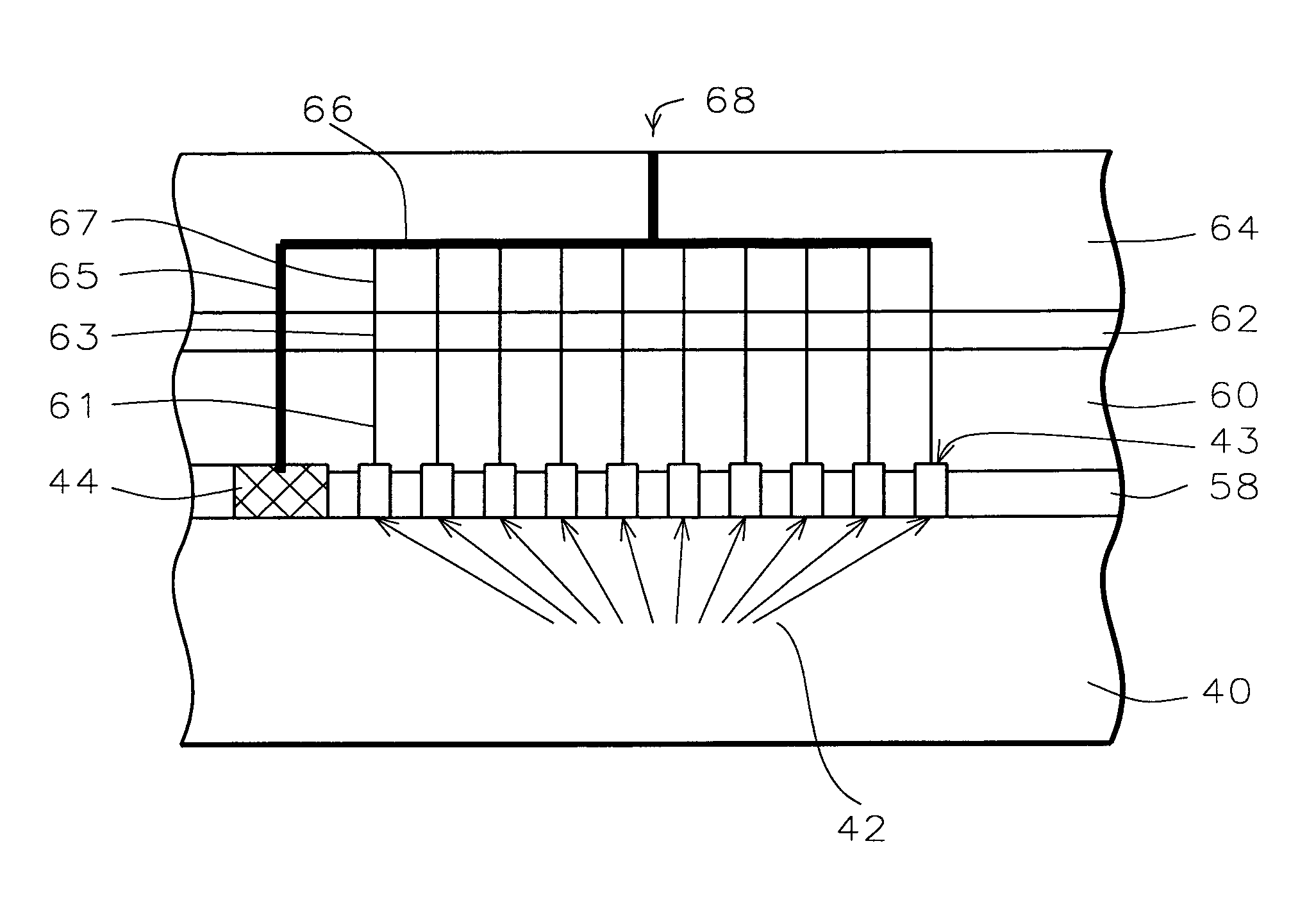
[0047]U.S. Pat. No. 6,383,916, teaches an Integrated Circuit structure where re-distribution and interconnect metal layers are created in layers of dielectric over the passivation layer of a conventional Integrated Circuit (IC). A layer of passivation is deposited over the IC, a thick layer of polymer is alternately deposited over the surface of the layer of passivation, and thick, wide metal lines are formed over the passivation.

[0048]Referring now more specifically to FIG. 6a, there is shown a cross section of one implementation of U.S. Pat. No. 6,383,916. The surface of silicon substrate 10 has been provided with transistors 11 and other devices (not shown in FIG. 6a). The surface of substrate 10 is covered by an interlevel dielectric (ILD) layer 12, formed over the devices.

[0049]Layers 14 (two examples are shown) represent all of the metal layers and dielectric layers that are typically created on the dielectric layer 12. Layers 14 contain multiple layers of dielectric or insula...


PUM


Abstract

A new method is provided for the creation of interconnect lines. Fine line interconnects are provided in a first layer of dielectric overlying semiconductor circuits that have been created in or on the surface of a substrate. A layer of passivation is deposited over the layer of dielectric, a thick second layer of dielectric is created over the surface of the layer of passivation. Thick and wide interconnect lines are created in the thick second layer of dielectric. The first layer of dielectric may also be eliminated, creating the wide thick interconnect network on the surface of the layer of passivation that has been deposited over the surface of a substrate.

Description

BACKGROUND OF THE INVENTION[0001](1) Field of the Invention[0002]The invention relates to the fabrication of integrated circuit devices, and more particularly, to a method of post-passivation processing for the creation of conductive interconnects.[0003](2) Description of the Prior Art[0004]Improvements in semiconductor device performance are typically obtained by scaling down the geometric dimensions of the Integrated Circuits; this results in a decrease in the cost per die while at the same time some aspects of semiconductor device performance are improved. The metal connections which connect the Integrated Circuit to other circuit or system components become of relative more importance and have, with the further miniaturization of the IC, an increasingly negative impact on the circuit performance. The parasitic capacitance and resistance of the metal interconnections increase, which degrades the chip performance significantly. Of most concern in this respect is the voltage drop a...

Claims


Application Information

Patent Timeline
Patent Type & Authority Patents(United States)
IPC IPC(8): H01L23/48H01L21/4763H01L21/768H01L23/528H01L23/532H01L23/60
CPCH01L23/5286H01L23/5329H01L23/60H01L27/0248H01L24/05H01L24/48H01L2224/05073H01L2224/05624H01L2924/01079H01L2924/05042H01L2924/14H01L2924/19041H01L2924/19042H01L2924/19043H01L2924/30105H01L2224/48H01L2924/01019H01L24/45H01L2224/45147H01L2924/00014
Inventor LIN, MOU-SHIUNG
Owner QUALCOMM INC
Why Eureka
Try Eureka