Method for manufacturing semiconductor integrated circuit

Active Publication Date: 2007-07-17
ELEMENT CAPITAL COMMERCIAL CO PTE LTD
View PDF35 Cites 34 Cited by
  • Summary
  • Abstract
  • Description
  • Claims
  • Application Information

AI Technical Summary

Benefits of technology

[0013]The present invention takes into consideration the above-mentioned circumstances, and it has as an object to solve the above problems generated when a semiconductor element is formed on an object having material properties different from those of the semiconductor element to improve the efficiency in using the semiconductor substra

Problems solved by technology

However, the improvements in signal transmittance rate in a bus has nearly reached its limit, and this has become a bottle neck in improving the processing rate of a computer.
However, since silicon is an indirect transition semiconductor, it cannot emit light by itself.
However, it is extremely difficult to directly form the VCSEL on a silicon integrated circuit using a semiconductor pr

Method used


Image

  • Method for manufacturing semiconductor integrated circuit
  • Method for manufacturing semiconductor integrated circuit
  • Method for manufacturing semiconductor integrated circuit

Examples


first embodiment

First Step:

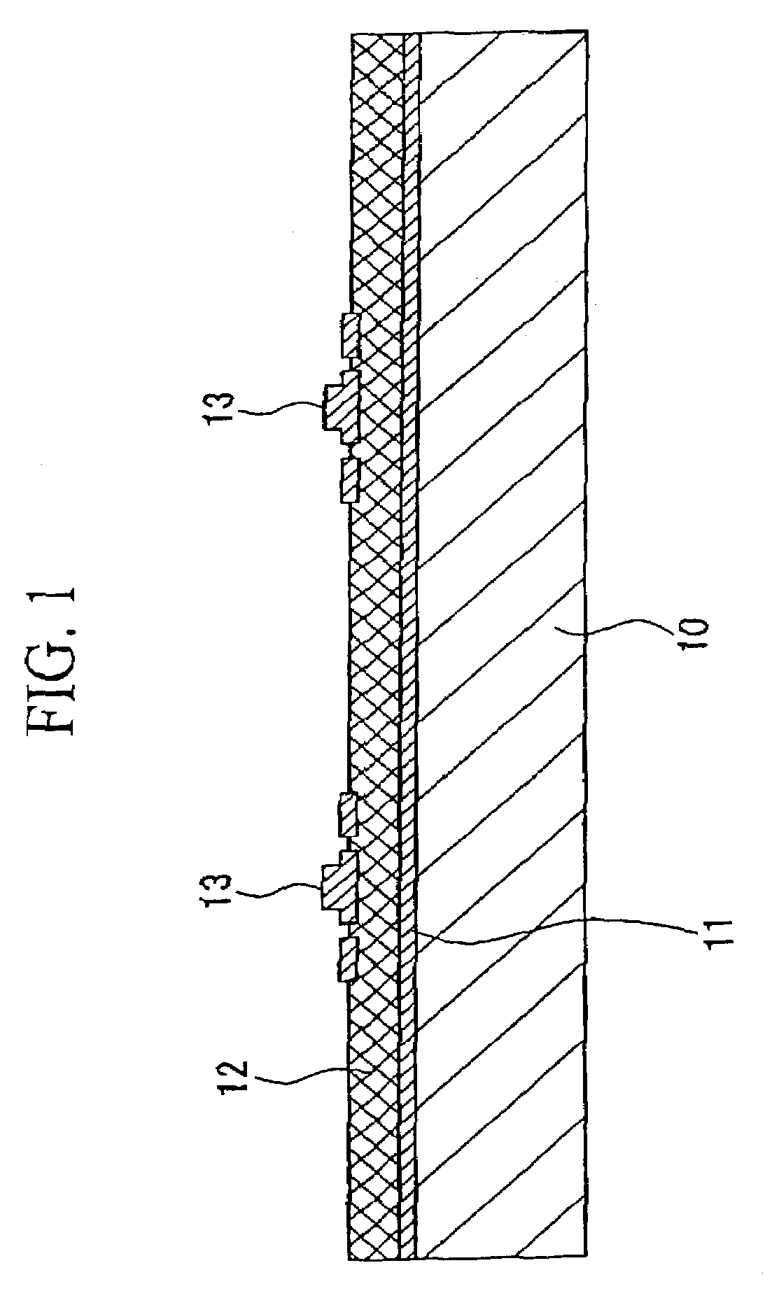
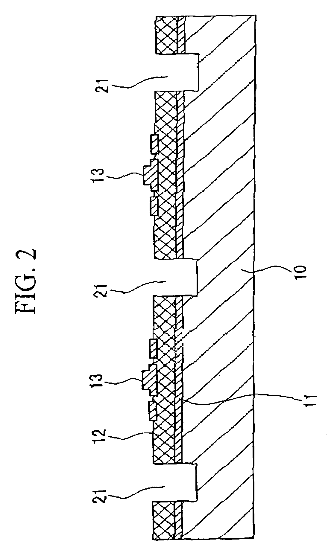
[0062]FIG. 1 is a diagram showing a schematic cross-sectional view for explaining the first step of a method for manufacturing a semiconductor integrated circuit according to the embodiment of the present invention. In FIG. 1, a substrate 10 is a semiconductor substrate, and in this embodiment, the substrate 10 is a GaAs compound semiconductor substrate. A sacrificial layer 11 is disposed as the lowest layer in the substrate 10. The sacrificial layer 11 is made of aluminum-arsenic (AlAs) and has a thickness of about several hundred nm, for example.

[0063]A functional layer 12 may be disposed on the sacrificial layer 11. The thickness of the functional layer 12 is, for instance, between about 1 to 20 μm. A semiconductor device (semiconductor element) 13 is formed on the functional layer 12. Examples of the semiconductor device 13 include, for instance, a light emitting diode (LED), a vertical cavity surface emitting laserdiode (VCSEL), a photodiode (PD), a high electron mob...

second embodiment

[0080]Next, in the second embodiment of the present invention, the case in which a silicon transistor (a silicon semiconductor element) is attached to a glass substrate for liquid crystal will be explained. The first to eleventh steps of the second embodiment correspond to the first to eleventh steps of the first embodiment. The significant difference between the first and second embodiments is that the method used for selectively etching the sacrificial layer in the fourth step is different.

[0081]In the first step of the second embodiment, a silicon transistor is formed on a silicon-on-insulator (SOI) substrate using an ordinary process. Here, it is possible to form an integrated circuit which is a silicon device, a photodiode, a transistor, or a diode instead of the silicon transistor. A silicon oxide membrane which becomes a sacrificial layer is provided with the SOI substrate.

[0082]In the second step, separation grooves are formed on the SOI substrate. Each separation groove has...


PUM


Abstract

A method for manufacturing a semiconductor integrated circuit includes steps of forming a semiconductor element on a semiconductor substrate and separating only a function layer including the semiconductor element, which is a surface layer of the semiconductor substrate, from the semiconductor substrate. The semiconductor element is preferably a compound semiconductor device including at least one of a light emitting diode, a vertical cavity surface emitting laserdiode, a photodiode, a high electron mobility transistor, an inductor, a capacitor, a resistor, and a heterojunction bipolar transistor.

Description

BACKGROUND OF THE INVENTION[0001]1. Field of the Invention[0002]The present invention relates to semiconductor integrated circuits, methods for manufacturing semiconductor integrated circuits, semiconductor element members, electrooptic devices, and electronic devices. More specifically, the present invention relates to a method for transferring a semiconductor element onto an object having material properties different from those of the semiconductor element, such as a substrate.[0003]2. Description of Related Art[0004]Techniques relating to the formation of a semiconductor element on a substrate, which has material properties different from those of the semiconductor element, have been proposed in the field. Such techniques include, for instance, formation of a vertical cavity surface emitting laserdiode (VCSEL), a photodiode (PD), or a high electron mobility transistor (HEMT) on a silicon semiconductor substrate, and attachment of a micro-silicon transistor, instead of a thin fil...

Claims


Application Information

Patent Timeline
IPC IPC(8): H01L21/46H01L21/331H01L21/02H01L21/20H01L21/306H01L21/336H01L21/338H01L21/60H01L27/12H01L27/15H01L29/737H01L29/778H01L29/786H01L29/812H01L51/52
CPCH01L21/2007H01L24/24H01L24/82H01L24/83H01L33/0079H01L2924/1305H01L2924/13064H01L2924/12041H01L2924/0132H01L2924/0105H01L2924/01006H01L2924/13063H01L2924/30105H01L2924/19043H01L2924/19042H01L2924/19041H01L2924/14H01L2924/10329H01L2924/01079H01L2924/01078H01L2924/01049H01L51/5237H01L51/5262H01L2221/68354H01L2221/68368H01L2224/24225H01L2224/24226H01L2224/32225H01L2224/83001H01L2224/83192H01L2224/838H01L2224/92H01L2224/92244H01L2924/01004H01L2924/01012H01L2924/01013H01L2924/01015H01L2924/01018H01L2924/01029H01L2924/01033H01L2924/01046H01L2924/01047H01L2224/83H01L2224/82H01L2924/01031H01L2924/3512H01L2924/00H01L2924/12043H01L33/0093H10K50/85H10K50/844
Inventor KONDO, TAKAYUKI
Owner ELEMENT CAPITAL COMMERCIAL CO PTE LTD
Why Eureka
Try Eureka