

Organic electro luminescent display and method for fabricating the same
a luminescent display and organic technology, applied in the manufacture of electrode systems, discharge tubes/lamps, electric discharge tubes/lamps, etc., can solve the problems of energy absorption rate, high possibility of damaging the pixel portion, and significantly low process accuracy, so as to achieve efficient selective removal of organic emissive layers, efficient cure
- Summary
- Abstract
- Description
- Claims
- Application Information
AI Technical Summary
Benefits of technology
Problems solved by technology
Method used
Image

Examples
first embodiment
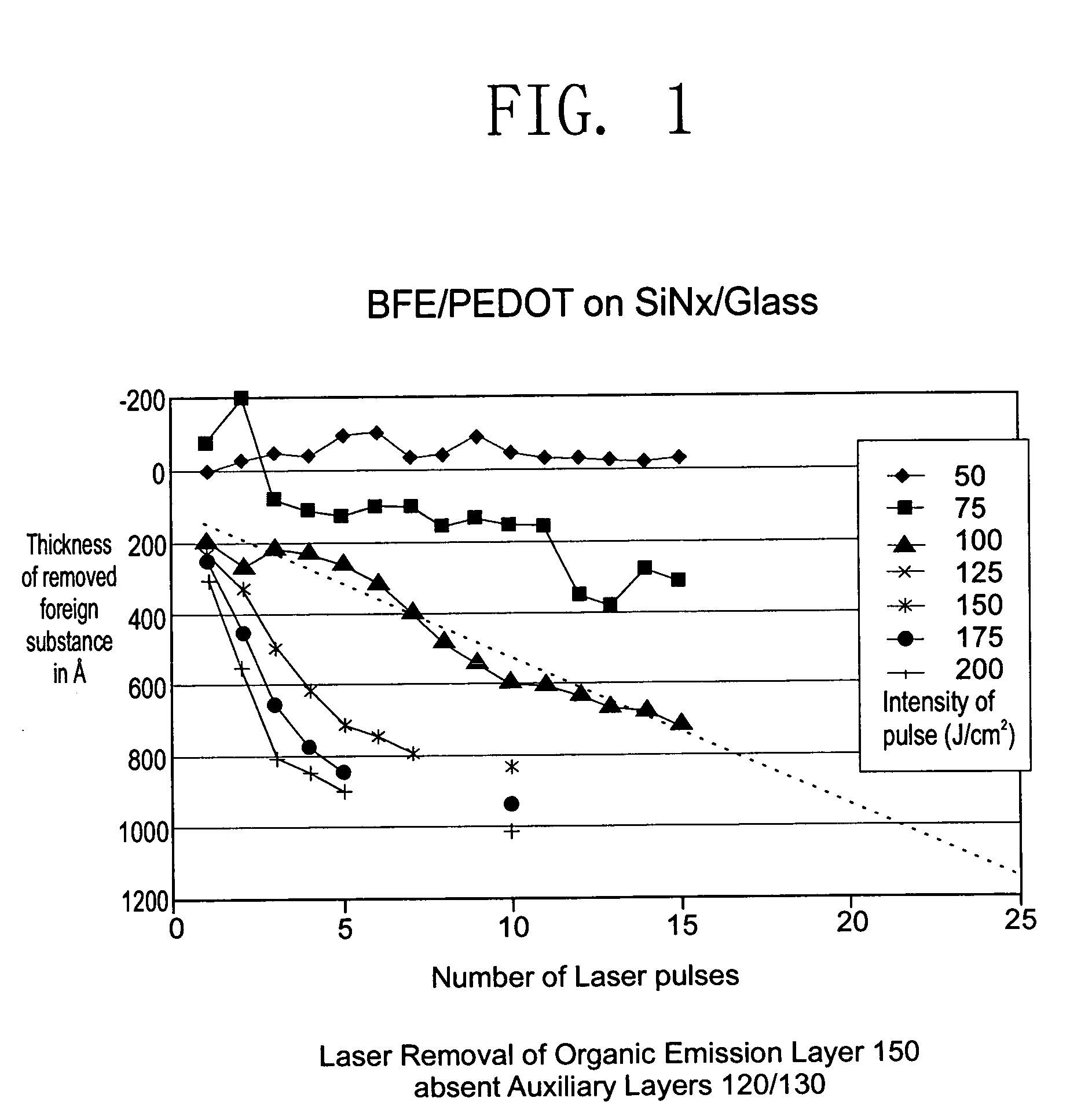
[0049
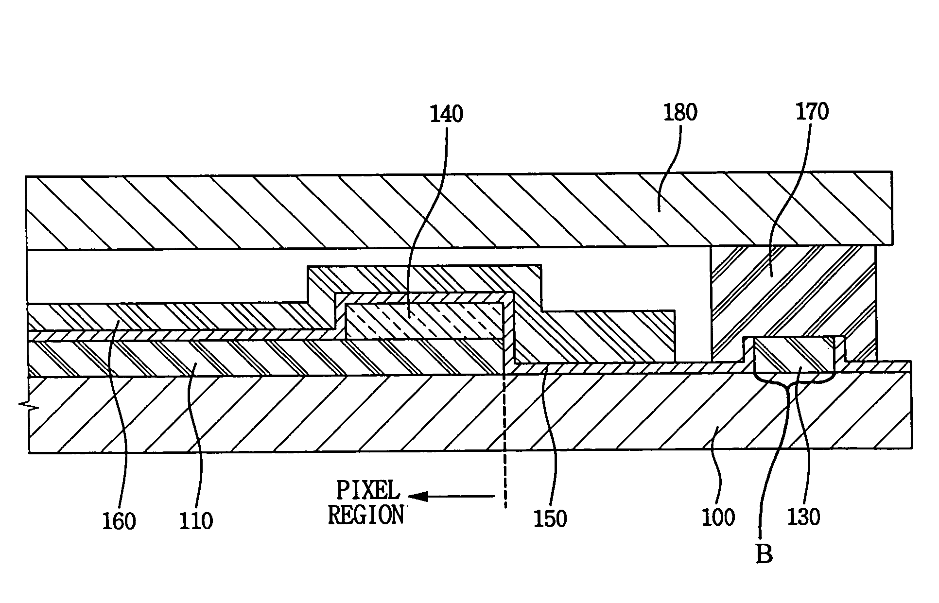
[0050]Turning now to FIG. 3, FIG. 3 is a plane view illustrating an organic electro luminescent display according to a first embodiment of the present invention, and FIGS. 4A to 4D are cross-sectional views illustrating a process for making the organic electro luminescent display of FIG. 3 according to an embodiment of the present invention.
[0051]Referring to FIG. 4A, a first electrode (or anode electrode) 1110 is deposited on substrate (or lower substrate) 1100. First electrode is made out of a transparent and conductive material such as ITO (indium tin oxide), IZO (indium zinc oxide) or ICO (indium cesium oxide). This transparent first electrode material is deposited and patterned on the lower insulating substrate 100, and a transparent anode electrode, in other words, the first electrode 1110 formed in the pixel portion. Lower substrate 100 may be a transparent substrate made out of an electrically insulating material, such as glass.
[0052]In the first embodiment, the auxilia...
second embodiment
[0061
[0062]The organic electro luminescent display according to a second embodiment has a similar structure as that of the first embodiment except the material used for the auxiliary layers 120 and 130 is different. In the second embodiment, the material used in the auxiliary layers 120 and 130 is the same as the material used in pixel defining layer 140. Therefore, pixel defining layer 140 and the auxiliary layers 120 and 130 can be formed at the same time. The pixel defining layer and the auxiliary layers are deposited at the same time and the patterning and etching of the pixel defining layer 140 and auxiliary layers 120 and 130 are accomplished in a single step. As discussed previously, the pixel defining layer 140 is preferably an inorganic material and a polymer such as an acrylic photoresist or a polyimide. By having the auxiliary layers 120 and 130 made out of the same material as the pixel defining layer 140, the number of pulses needed and the energy intensity of each puls...
third embodiment
[0063
[0064]The organic electro luminescent display according to a third embodiment has a similar structure as that of the first embodiment except that the auxiliary layers 120 and 130 for removing the organic layers 150 are formed by using materials having a laser energy absorption rate higher than that of the organic layer 150 for the laser wavelength used to remove the organic layer.
[0065]That is, after forming the pixel defining layer 140 in the first embodiment, the auxiliary layers 120 and 130 are formed on the cathode contact A and the encapsulating junction region B by depositing and patterning materials having a higher laser energy absorption rate for the laser wavelength used in the removal process
[0066]The third embodiment is not necessarily mutually exclusive from the first or the second embodiment. For example, use of ITO, IZO or ICO could result in the auxiliary layer having a higher absorption of the laser light than the organic layer and thus the auxiliary layers 120 ...
PUM
 Abstract
Description
Claims
Application Information