Semiconductor device, and method and apparatus for manufacturing semiconductor device

a semiconductor and manufacturing method technology, applied in the direction of sustainable manufacturing/processing, gated amplifiers, final product manufacturing, etc., can solve the problems of high price and difficulty in urgent procurement, variable impedance, and large external dimensions of air core coils, so as to achieve accurate and secure packaging, improve packaging yield, and improve the effect of efficiency

Inactive Publication Date: 2007-08-28
HITACHI LTD +2
View PDF15 Cites 13 Cited by
  • Summary
  • Abstract
  • Description
  • Claims
  • Application Information

AI Technical Summary

Benefits of technology

[0063]① Among the electronic components to be mounted over the module substrate, the air core coil is the highest, but it is packaged after all the other electronic components have been mounted. Therefore, the collet holding the air core coil by vacuum suction does not come into contact with the electronic components already mounted over the module substrate or damage other electronic components. This can mean an improved packaging yield.
[0064]② After the leading one of the air core coils, shifted to the bulk feed section bulk feeder and aligned in tandem, is held by the collet by vacuum suction, it is carried to a prescribed position over the module substrate and, though after that it is fixed by melting solder provided in advance on the module substrate and the air core coil by temporary heating, in the bulk feed section the leading air core coil is fed separately from the following air core coil. Accordingly, there can occur no error in vacuum suction holding by the collet which would otherwise occur as the following air core coil overlaps or is caught by the leading air core coil, resulting in accurate and secure packaging, which moreover can be carried out more efficiently. Therefore, the process is made less susceptible to packaging faults or machinery stopping, making it possible to reduce the packaging cost.
[0065]③ As the wall of the cylindrical feed shaft is thin in the hopper portion, the bulk will not ride on and stop the shaft, and the air core coil to the bulk feed section is made more secure, making possible stable feeding.
[0066]④ As the positional relationship in the hopper portion is such that, in a state in which the guide is at its lowest, there can arise no gap between the outer circumference of the feed shaft and the frustum concave face of the guide in which the bulk could be held, there is no possibility for an air core coil to be caught between the outer circumference of the feed shaft and the frustum concave face of the guide. Therefore, the air core coils can be prevented from deformation or any deformed air core coil from being mounted, making possible an improvement in packaging yield. It is also made possible to stably feed the bulk feed section with air core coils.

Problems solved by technology

In addition, portable devices in particular require consideration for the resistance of amplifying element of the final stage (semiconductor amplifying element) against a high voltage that may work on it as a result of reflection that would result from a substantial variation in the impedance of the antenna and consequent load mismatching.
Thus, chip inductors require a current capacity of 2 A or more when they are to be used on the power supply line of a high frequency power amplifying device, and therefore have to be produced to a special specification, which means a correspondingly high price and difficulty of urgent procurement.
Commercially available air core coils are too large in external dimensions to be mounted on a module which has a prescribed height limit.
Moreover, conventional chip inductors are expensive, and their high prices constitute a constraint to cost reduction of hybrid integrated circuit devices.
However, the applicants have found that it is difficult to stably supply such extremely light coils (air core coils) with the conventional bulk feeder.

Method used


Image

  • Semiconductor device, and method and apparatus for manufacturing semiconductor device
  • Semiconductor device, and method and apparatus for manufacturing semiconductor device
  • Semiconductor device, and method and apparatus for manufacturing semiconductor device

Examples


embodiment 1

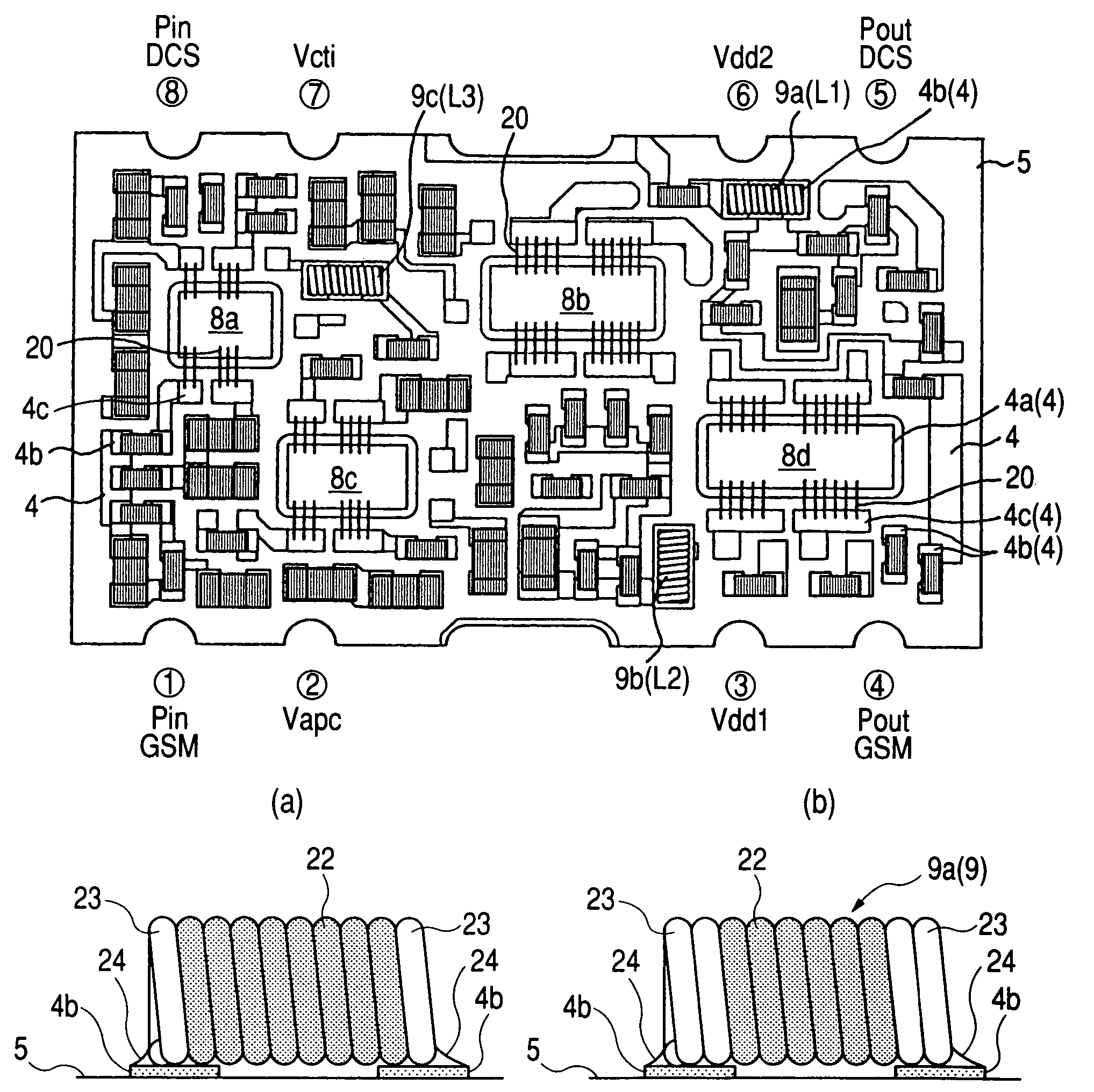
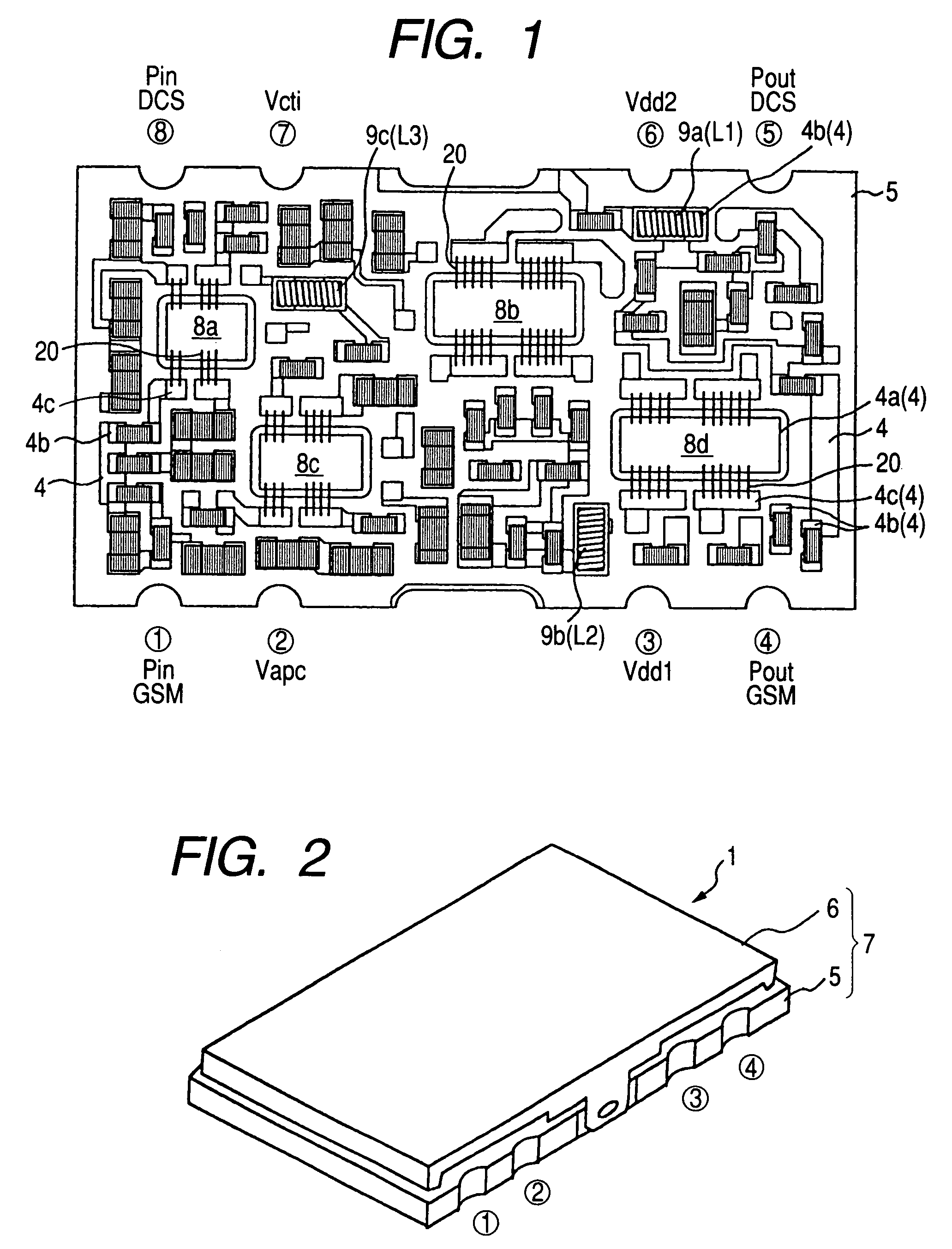
[0128]FIG. 1 through FIG. 31 pertain to a semiconductor device (high frequency power amplifying device), which is a preferred embodiment of the invention (Embodiment 1) together with a manufacturing method therefor, and a wireless communication device (electronic device)

[0129]This Embodiment 1 described below is a case in which the invention is applied to a high frequency power amplifying device (hybrid integrated circuit device) as a semiconductor device. The high frequency power amplifying device, which is this Embodiment 1, is for dual band use, for instance a dual band high frequency power amplifying device built into a mobile telephone (wireless communication device), into which a GSM communication system and a DCS communication system are incorporated.

[0130]A high frequency power amplifying device (high frequency power amplifier module) 1 in this Embodiment 1 is a flat rectangular structure in external view as shown in FIG. 2. This high frequency power amplifying device 1 has ...

embodiment 2

[0231]FIG. 32 shows a partial typical view of part of the bulk feeder 21, which is another preferred embodiment of the invention (Embodiment 2). As shown in FIG. 32, there is provided an air feed path 49 communicating with the pipe 35. This air feed path 49 communicates to the guide hole 17 of the feed shaft 18 and, as shown in FIG. 32, blows air into guide hole 17. This enables any clogging of the guide hole 17 with an air core coil 9 to be easily eliminated.

embodiment 3

[0232]FIG. 45 through FIG. 54 pertain to the manufacture of a high frequency power amplifying module, which is another preferred embodiment of the invention (Embodiment 3).

[0233]This Embodiment 3 concerns a technique by which coils (air core coils) can be mounted over a module substrate without deviation in positioning.

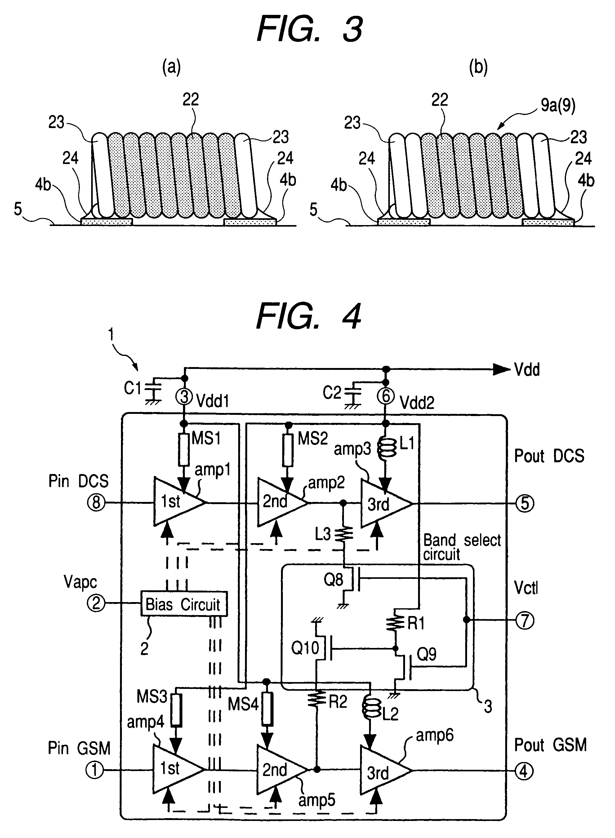
[0234]In mounting an air core coil, electrodes at the both ends of the air core coil are superposed over electrode fixing pads on the module substrate, followed by fixing of the electrode portions onto the electrode fixing pads by reflowing solder applied in advance over the surfaces of the electrode fixing pads. It was found that, in this fixing process, there might occur a faulty phenomenon that the air core coil 9 deviates from its due position as shown in FIG. 52(c). Even if the electrodes 23 of the air core coil 9 are correctly superposed over the electrode fixing pads 4b provided on the surface of the module substrate 5, positional deviation may occur during the...


PUM

PropertyMeasurementUnit
inner diameteraaaaaaaaaa
current capacityaaaaaaaaaa

Abstract

A high frequency power amplifying device has two amplifying lines. Each amplifying line has a configuration in which a plurality of amplifying stages are connected in cascade having two source voltage terminals, of which one is connected to the first amplifying stage of one amplifying line and to the remaining amplifying stages of the other amplifying line, and the other, to the first amplifying stage of the latter amplifying line and to the remaining amplifying stages of the former amplifying line. An air core coil with a low D.C. resistance, formed by spirally winding a copper wire of about 0.1 mm in diameter, is connected in series between the final amplifying stage of each amplifying line and the source voltage terminal.

Description

TECHNICAL FIELD[0001]The present invention relates to a semiconductor device, a manufacturing method therefor and a semiconductor manufacturing apparatus, and more particularly, for instance, to a manufacturing technique for a multi-stage high frequency power amplifying device (high frequency power amplifying module) in which a plurality of amplifiers (semiconductor amplifying elements) are connected in cascade in multiple stages as a semiconductor device, and a technique that can be effectively applied to a wireless communication device (electronic device) into which the high frequency power amplifying device is incorporated, such as a mobile telephone.BACKGROUND ART[0002]A high frequency power amplifying device for use in wireless communication devices, such as car telephones or mobile telephones, has a multi-stage configuration in which a plurality of amplifiers, each consisting of a semiconductor amplifying element (transistor), are connected in cascade in two, three or more sta...

Claims


Application Information

Patent Timeline
Patent Type & Authority Patents(United States)
IPC IPC(8): H01L29/00H01L25/04H01F17/02H01F27/29H01L23/64H01L23/66H03F3/60H03F3/72H04B1/04H05K1/18H05K13/02
CPCH01F17/02H01F27/292H05K13/028H05K1/181H01L23/645H01L23/66H03F3/602H03F3/72H01L2924/01047H01L2924/01015H01L2924/12041H01L2224/45147H01L24/49H01L24/48H04B2001/0408H03F2203/7236H01L2223/6644H01L2224/48227H01L2224/49175H01L2924/01012H01L2924/01046H01L2924/01078H01L2924/09701H01L2924/14H01L2924/15313H01L2924/19041H01L2924/19104H01L2924/19105H01L2924/30107H01L2924/3011H01L2924/3025H03F2200/429H01L2924/00H01L2224/45015H01L2924/00014H01L2924/12042H01L24/45H03F3/24Y02P70/50H01L2924/2076H01L2224/05599H01L25/04
Inventor KYOGOKU, TOSHIHIKOKODU, TADASHIMOCHIDUKI, KIYOHARUKIKUCHI, SAKAEISHIDU, AKIOKOBAYASHI, YOSHIHIKOMARUYAMA, MASASHIKOJIRO, IWAMICHISATO, SUSUMU
Owner HITACHI LTD
Why Eureka
Try Eureka