Booster circuit and semiconductor device having same

a booster circuit and semiconductor technology, applied in the direction of electric variable regulation, process and machine control, instruments, etc., can solve the problems of the inability to meet the phase lag, and the inability to control the peak current at start-up, so as to achieve lower power supply voltage, higher speed, and the effect of reducing the voltage of the power supply

Inactive Publication Date: 2007-09-25
RENESAS ELECTRONICS CORP
View PDF8 Cites 29 Cited by
  • Summary
  • Abstract
  • Description
  • Claims
  • Application Information

AI Technical Summary

Benefits of technology

[0011]Accordingly, an object of the present invention is to provide a booster circuit in which by controlling start-up of charge pump units in accordance with boosted voltage, peak consumption current of the booster circuit is suppressed and efficiency of consumed current with respect to boosted voltage is improved, as well as a semiconductor device equipped with such booster circuits.
[0022]The present invention is capable of providing a booster circuit in which by successively activating a plurality of charge pump units in accordance with a boosted voltage by monitoring the boosted voltage, peak consumption current is suppressed and each of the charge pump units is operated in a state in which the efficiency of consumed current with respect to the boosted voltage is high. The present invention also provides an ideal semiconductor device equipped with such booster circuits.

Problems solved by technology

With the above-described method of staggering the phases of the clock pulses, a satisfactory phase lag cannot be set.
A problem which 3arises is that peak current at start-up and fluctuation of the power supply voltage cannot be controlled.

Method used


Image

  • Booster circuit and semiconductor device having same
  • Booster circuit and semiconductor device having same
  • Booster circuit and semiconductor device having same

Examples


first embodiment

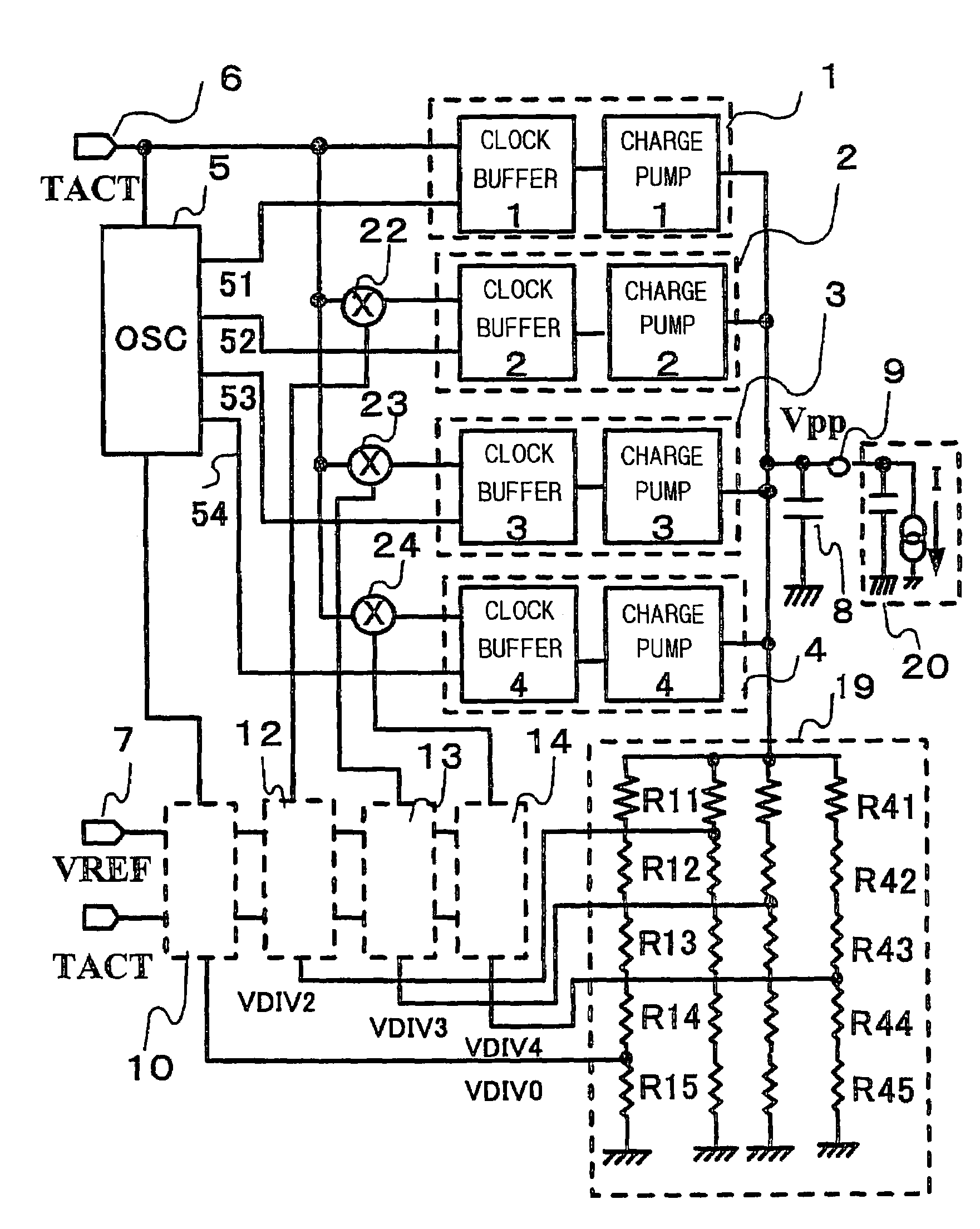
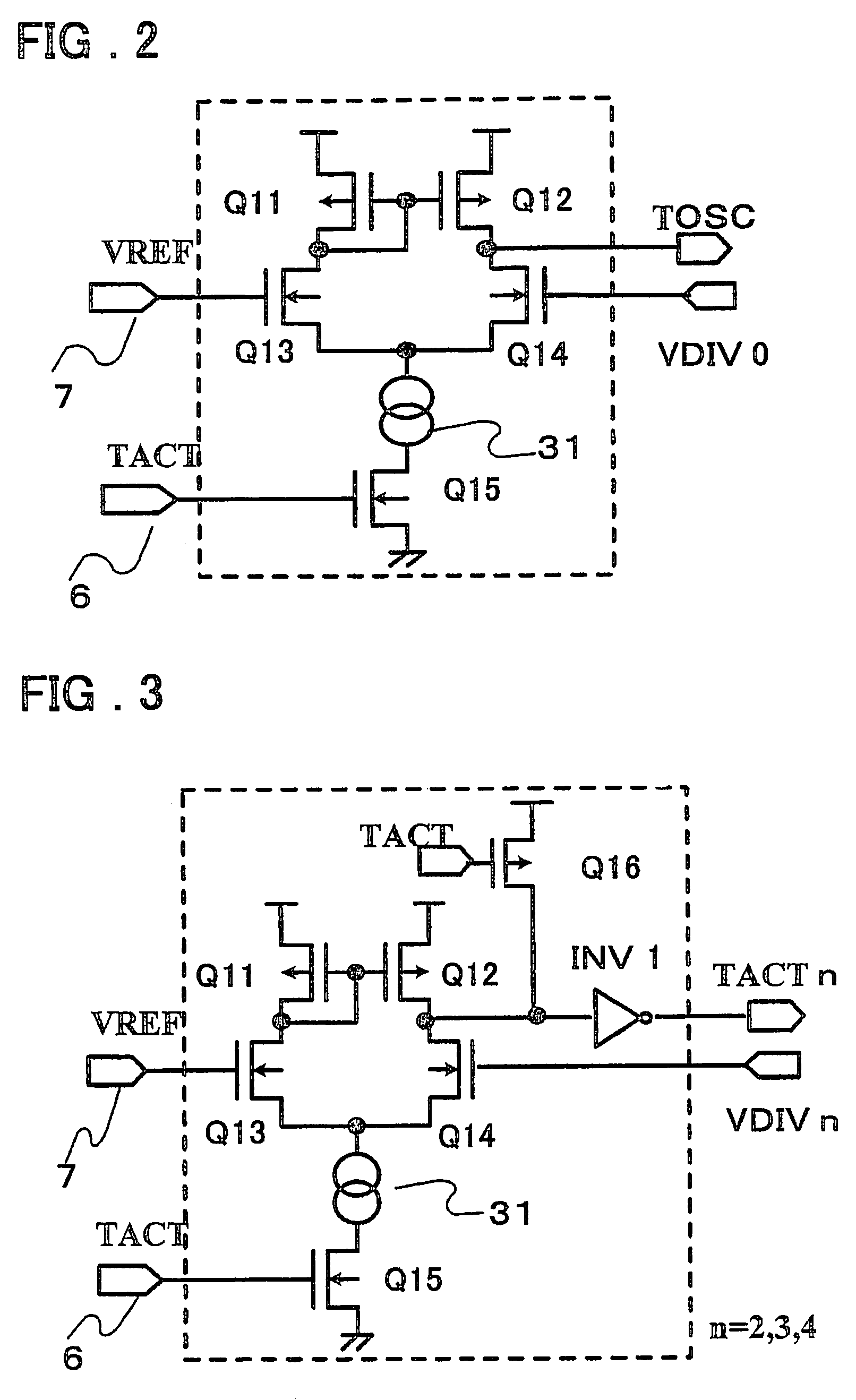
[0033]FIG. 1 is a circuit block diagram illustrating a booster circuit according to a first embodiment of the prior art, FIG. 2 is a circuit diagram of first comparison unit, FIG. 3 is a circuit diagram of second comparison unit, FIG. 4 is a circuit diagram illustrating a changeover device for changing over a clock buffer control signal, and FIG. 5 is a timing chart illustrating operation.

[0034]The booster circuit shown in FIG. 1 comprises charge pump units 1 having a clock buffer #1 and a charge pump circuit #1; charge pump unit 2, 3 and 4 similarly having clock buffers #2, #3 and #4 and charge pump circuits #2, #3 and #4, respectively; a clock generating circuit 5 for generating a basic clock 51 and clocks 52, 53 and 54 each of which is shifted in phase relative to the basic clock; a capacitor 8; voltage dividing unit 19 for dividing a boosted voltage; comparison units 10, 12, 13 and 14; and control signal changeover devices 22, 23 and 24. The booster circuit has an input terminal...

second embodiment

[0070]FIG. 6 illustrates the circuit structure of second voltage dividing unit for dividing boosted voltage in a second embodiment of the present invention. In the second embodiment, the voltage dividing unit of the first embodiment for dividing boosted voltage and outputting the divided boosted voltage is modified to have the structure shown in FIG. 6. This embodiment is such that when the boosted voltage has declined owing to supply of current to the load of the booster circuit, a charge pump unit, once it has starting the boosting operation, is prevented from suspending the boosting operation and is allowed to continue performing boosting.

[0071]In comparison with the voltage dividing unit 19 for dividing boosted voltage in FIG. 1, it will be understood that the voltage dividing unit of this embodiment differs in that the second, third and fourth resistor groups are each additionally provided with a transistor and an inverter. Structural elements identical with those of FIG. 1 are...

third embodiment

[0081]FIG. 7 illustrates a third embodiment of the present invention. The embodiment in FIG. 7 differs in the arrangement of the comparison units and voltage dividing units that outputs divided boosted voltage. Structural elements identical with those in FIG. 1 are designated by like reference characters and need not be described again. The voltage dividing unit for outputting divided boosted voltage comprises resistors R51 and R52, with divided boosted voltage VDIV1 being output from the node of resistors R51 and R52. Comparison units 15, 16, 17 and 18 compare the commonly applied divided boosted voltage with different reference voltages 71 to 74, and output clock generation control signals or charge pump control signals.

[0082]In the comparison means of the first embodiment shown in FIG. 1, a common reference voltage is applied to these comparison units, which compare the reference voltage with respective ones, respectively, of divided boosted voltages having voltage values that di...


PUM


Abstract

A booster circuit for boosting an externally supplied voltage includes a plurality of parallel-connected charge pump units. The charge pump units are activated successively in accordance with a boosted voltage to suppress peak current at start-up of the booster circuit and reduce fluctuation of power supply voltage.

Description

FIELD OF THE INVENTION[0001]This invention relates to a booster circuit for boosting power supply voltage supplied from an external source and generating a boosted voltage, and to a semiconductor device equipped such booster circuits.BACKGROUND OF THE INVENTION[0002]Conventionally, a semiconductor device such as a flash memory or dynamic memory is such that the voltage necessary for internal operation is generated within the semiconductor device so that such operations as write, read and erase of stored content may be performed. To accomplish this, the semiconductor device is provided internally with a booster circuit that includes charge pump units. A problem encountered, however, is a large peak consumption current that develops in the booster circuit at the time of start-up and a power supply voltage that fluctuates. Many improvements have been made heretofore.[0003]An example of such an improvement is to reduce the voltage amplitude of a boot-up signal immediately after input of...

Claims


Application Information

Patent Timeline
Patent Type & Authority Patents(United States)
IPC IPC(8): G05F1/10G11C16/06G11C11/407H01L27/04H02M3/07
CPCG11C5/145H02M1/36H02M3/073H02M2003/077H02M3/077
Inventor OKAMOTO, TOSHIHARU
Owner RENESAS ELECTRONICS CORP
Why Eureka
Try Eureka