Half-wavelength micropost microcavity with electric field maximum in the high-refractive-index material

a micropost microcavity and high-refractive index material technology, applied in the field of optical devices and components, can solve the problems of large volume v, inconvenient design, and inability to relocate the active layer to the field maximum

Inactive Publication Date: 2007-11-06
THE BOARD OF TRUSTEES OF THE LELAND STANFORD JUNIOR UNIV
View PDF2 Cites 6 Cited by
  • Summary
  • Abstract
  • Description
  • Claims
  • Application Information

AI Technical Summary

Benefits of technology

[0010]The devices of the present invention operate with an electric field intensity maximum at the center of the cavity where the active layer is located, thus providing strong interaction between the cavity field and the active layer. At the same time, the devices provide a high-refractive-index material at the center of the cavity, thus enabling the active layer to be embedded at the center of the cavity, where the field intensity is maximum. The devices also provide an increase in the ratio Q / V relative to all previously known microposts.

Problems solved by technology

However, although the Q factor for this design is high, it has the disadvantage that the mode volume V is large due to the wavelength-thick spacer region, and this large mode volume offsets the high quality factor.
Because the electric field will not interact with the active layer, this design is not useful.
Moreover, it is impossible to relocate the active layer to the field maximum, as the maximum is in the low index material.
Because the active layer (e.g., quantum dot or quantum well) needs to be embedded in the high refractive index material, as explained previously, this design is not useful.
If the mode volume is decreased by using a half-wavelength spacer, however, the resulting device either has a minimum field intensity at the center of the spacer, as shown in FIG. 2b, or has a spacer with a low refractive index that is not suitable for an embedding active layer, as shown in FIG. 3b.
Thus, according to conventional design principles known in the art, it is not possible to obtain a micropost microcavity device that has a maximum field intensity at the center of a high-index spacer whose thickness is half a wavelength, i.e., it is impossible to locate an active layer at the field maximum of the device with half-wavelength spacer (of either low or high-index).
Consequently, although it is desirable to design microcavity devices with higher Q / V values, the design trade-offs have prevented the realization of this goal.

Method used


Image

  • Half-wavelength micropost microcavity with electric field maximum in the high-refractive-index material
  • Half-wavelength micropost microcavity with electric field maximum in the high-refractive-index material
  • Half-wavelength micropost microcavity with electric field maximum in the high-refractive-index material

Examples


Embodiment Construction

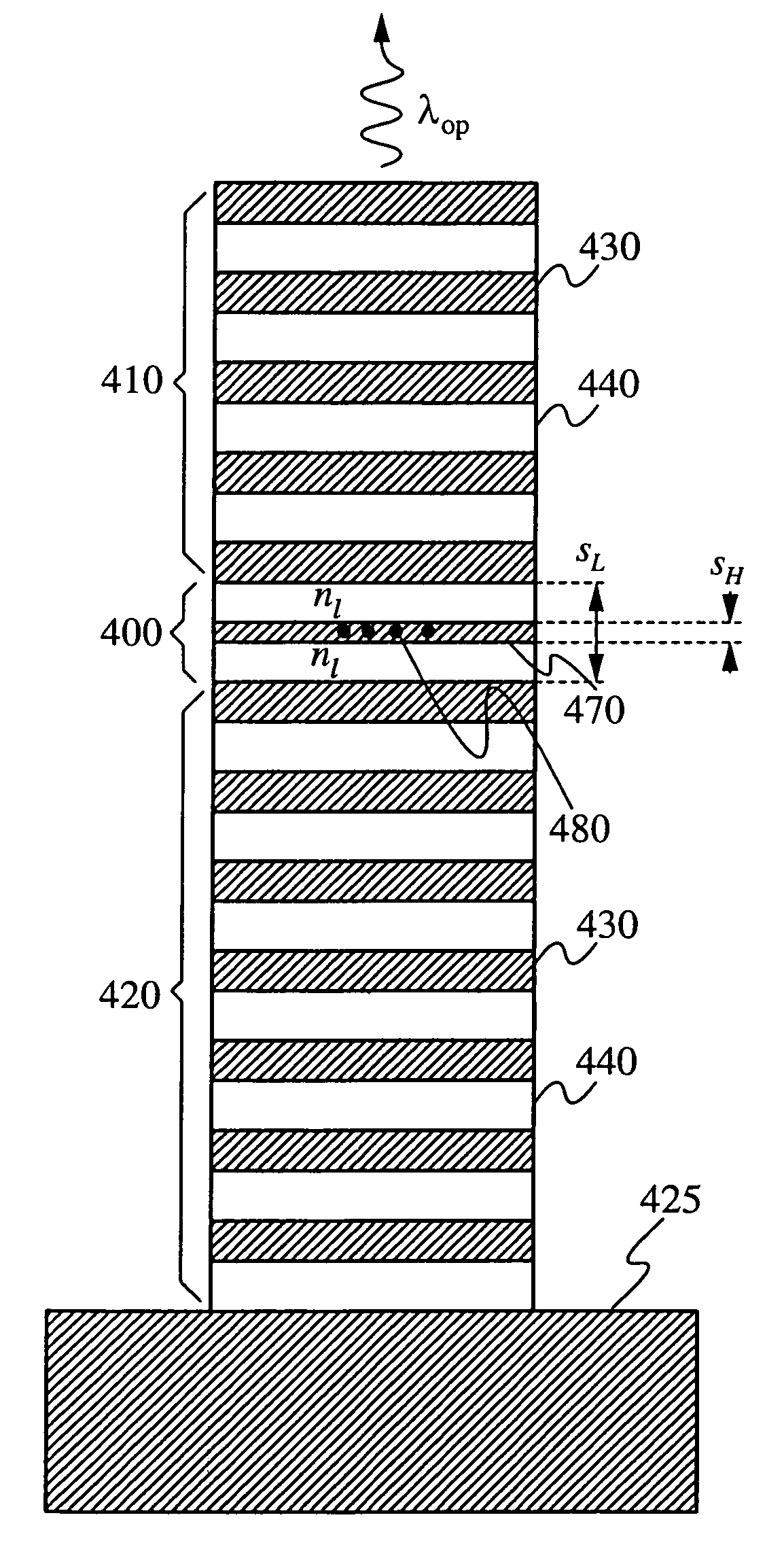
[0019]One embodiment of a micropost microcavity according to the invention is shown in FIG. 4a. The device of finite diameter is designed to operate at a predetermined operational wavelength, λop400 is sandwiched between two dielectric mirrors 410 and 420, and the device may be fabricated on a substrate layer 425 using conventional fabrication processes. Dielectric mirrors 410, 420 are distributed-Bragg-reflectors (DBRs), constructed by stacking alternating high-refractive index layers 430 and low-refractive index layers 440 on top of each other. The low index layers 440 are composed of a material having a refractive index nl, while the high index layers 430 are composed of a material having a refractive index nh, where nlh. The alternating low index and high index layers have alternating quarter-wave thicknesses λ / 4nl and λ / 4nh, respectively. The mirrors are optimized for the planar case rather than for the actual operating wavelength.

[0020]As is well known in the art, many materia...


PUM


Abstract

A micropost microcavity device has a maximum field intensity at the center of a high-index spacer as well as a small mode volume. The device has an approximately half-wavelength thick low-index spacer [400] sandwiched between two quarter wave stacks [410, 420]. The low-index spacer has a high-index subspacer layer [470] positioned at its center. The subspacer layer has a thickness smaller than a quarter wavelength. As a result, the electric field intensity remains a maximum at the center of the spacer where the high-index subspacer is positioned. A quantum dot or other active region [480] may be embedded within the subspacer [470]. The microcavity devices provide, for example, single photon sources, single dot lasers, low-threshold quantum dot or quantum well lasers, or devices for strong coupling between a single quantum dot and the cavity field which can be used as components of photonic integrated circuits, quantum computers, quantum networks, or quantum cryptographic systems.

Description

CROSS-REFERENCE TO RELATED APPLICATIONS[0001]This application claims priority from U.S. provisional patent application 60 / 399,913 filed Jul. 30, 2002, which is incorporated herein by reference.FIELD OF THE INVENTION[0002]The present invention relates generally to optical devices and components. More specifically, it relates to photonic crystal microcavities, distributed-Bragg-reflector micropost microcavities, and related devices.BACKGROUND OF THE INVENTION[0003]Photonic crystal microcavities exhibiting cavity quantum electrodynamic (QED) phenomena can be used to construct optical devices such as high-efficiency light emitting diodes, low-threshold lasers, and single photon sources. During the growth process of a solid-state microcavity, a single narrow-linewidth emitter (quantum dot) can be embedded in the device, enabling cavity-field interaction with the quantum dot. The coupling between the quantum dot and the electric field in the cavity enhances the radiative transition rate o...

Claims


Application Information

Patent Timeline
Patent Type & Authority Patents(United States)
IPC IPC(8): H01S5/00G02BH01S5/183G06N99/00H01S5/32H01S5/34
CPCB82Y10/00B82Y20/00G06N99/002H01S5/3412H01S5/1042H01S5/18358G06N10/00G06N10/40
Inventor VUCKOVIC, JELENAYAMAMOTO, YOSHIHISA
Owner THE BOARD OF TRUSTEES OF THE LELAND STANFORD JUNIOR UNIV
Why Eureka
Try Eureka