FinFET transistor device on SOI and method of fabrication

a transistor and soi technology, applied in the field of finfet technology, can solve the problems of increasing the leakage current through channels, junctions, gate dielectrics, and conventional cmos devices with short gate lengths or nodes, and achieve the effect of reducing contact resistance, reducing channel resistance, and thin body

Active Publication Date: 2007-11-27
TAIWAN SEMICON MFG CO LTD
View PDF3 Cites 155 Cited by
  • Summary
  • Abstract
  • Description
  • Claims
  • Application Information

AI Technical Summary

Benefits of technology

[0054]In another embodiment of the present invention, at least two fins having a narrow thickness of about 6.5 nm and a pitch of 0.25 μm defining two channels is provided that allows the device to perform with the advantages of “thin body” effects. The raised source pad and drain pad reduce contact resistance.
[0055]The raised source and drain pads operate to reduce channel resistance. Additionally, the raised source and drain pads eliminate the need for a top mask or passivation layer to be deposited on top of the source and drain regions of the FinFET transistor device of the present invention.

Problems solved by technology

Additionally, as CMOS on bulk silicon devices are scaled to channel lengths below 100 nm, conventional CMOS devices suffer from several problems.
For example, conventional planar complementary metal oxide semiconductor (CMOS) technology on bulk silicon having a short gate length or node, such as 90 nm or 65 nm, suffers from a degraded performance, including increased leakage currents that occur through channels, junctions, and gate dielectrics.
In particular, interactions between the source and drain of the CMOS device typically results in both Vt roll-off and sub-threshold swing, degrading the ability of the gate of the device to control whether the device is on or off.
As device size is scaled, however, this becomes increasingly difficult, since the distance between the source and drain is reduced, and hence, both the source and the drain increasingly interact with the channel, thus reducing gate control and increasing short channel effects (SCE).
However, the throughput of E-beam lithography is low and the uniformity is not satisfactory for a sub-30 nm gate length device.
The SOI layer not only reduces the capacitance of the semiconductor switch so it operates faster, but also eliminates the “body effect” which causes lower current and lower performance in CMOS on bulk technology.
However, narrow fin widths can cause high channel resistance in DG FinFET on SOI devices.

Method used


Image

  • FinFET transistor device on SOI and method of fabrication
  • FinFET transistor device on SOI and method of fabrication
  • FinFET transistor device on SOI and method of fabrication

Examples


Embodiment Construction

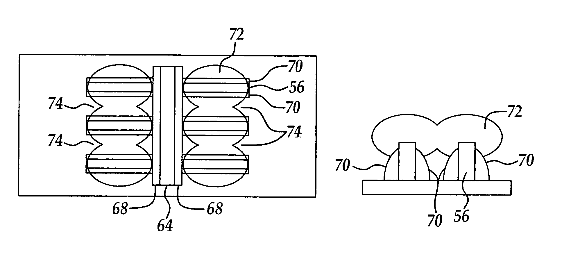
[0086]Generally, the present invention provides a novel FinFET transistor on SOI device and method of fabrication. The present invention defines at least two FinFET transistor fins each having an upper poly-silicate glass portion and a lower silicon portion using a spacer patterning technology. Each fin is formed by patterning a sacrificial SiN mask with a sacrificial support structure, wherein a CVD pad oxide is first deposited underneath the SiN mask on a top silicon layer of a SOI substrate. The SiN hard mask is removed and then a breakthrough etch is applied to remove the pad oxide below the SiN layer. The final fin formation step provides forming an oxide hard mask and using an etch to define at least two, and preferably, multiple fins having a close fin pitch, preferably about 0.25 μm. Each fin is called a “spacer”.

[0087]After the fins or spacers are formed, selective epitaxy is used to form a raised source-drain, wherein each raised source-drain associated with each fin will ...


PUM


Abstract

A FinFET transistor on SOI device and method of fabrication is provided. At least two FinFET fins each having an upper poly-silicate glass portion and a lower silicon portion are formed using spacer patterning technology. Each fin is formed on a sacrificial SiN mask layer having a sacrificial support structure. The SiN mask is removed and then a breakthrough etch is applied to remove an underlying pad oxide layer. A PSG layer defining a width of each of the fins on a sidewall of each of the support structures is deposited on each of the support structures. At least two fins each having a narrow fin pitch of about 0.25 μm. are formed. The fins provide a seed layer for at least two selective epitaxially raised source and drain regions, wherein each raised source-drain associated with each fin are interconnected thus forming a source pad and a drain pad.

Description

FIELD OF THE INVENTION[0001]The present invention generally relates to FinFET technology and more particularly, relates to a FinFET transistor device on SOI and associated fabrication methods.BACKGROUND[0002]Performance enhancement between generations of integrated circuit devices is generally achieved by reducing the size of the device, resulting in an enhancement in device speed. This is generally referred to as device “scaling”. As scaling increases, to achieve faster device speeds using transistor IC technology, shorter gate lengths, thinner gate oxides and faster response times are necessary.[0003]Metal-oxide-Semiconductor-Field-Effect-transistors, MOSFETs, having a source, a drain region, and a gate electrode formed using a gate oxide, are commonly used in IC devices. As the gate oxide becomes thinner, the device must be powered with a lower voltage power supply to avoid breakdowns and leakage.[0004]Additionally, as CMOS on bulk silicon devices are scaled to channel lengths be...

Claims


Application Information

Patent Timeline
Patent Type & Authority Patents(United States)
IPC IPC(8): H01L21/8238H01L21/336H01L29/78H01L29/786
CPCH01L29/66628H01L29/785H01L29/66795H01L29/7854
Inventor CHEN, HAU-YUCHANG, CHANG-YUNHUANG, CHENG-CHUNGYANG, FU-LIANG
Owner TAIWAN SEMICON MFG CO LTD
Why Eureka
Try Eureka