
Nano-drive for high resolution positioning and for positioning of a multi-point probe

a technology of nano-drives and probes, applied in electrical testing, electronic circuit testing, instruments, etc., can solve problems such as inferior physical contact of one tip

Inactive Publication Date: 2007-12-04
CAPRES
View PDF33 Cites 27 Cited by
  • Summary
  • Abstract
  • Description
  • Claims
  • Application Information

AI Technical Summary

Benefits of technology

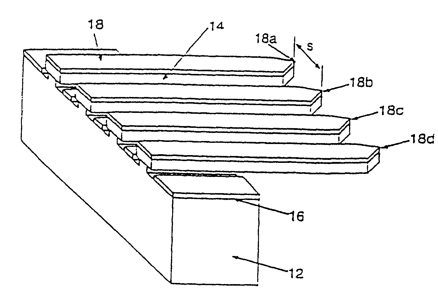
[0014]A particular advantage of the present invention is related to the fact that the novel testing technique involving a novel multi-point probe allows the probe to be utilised for establishing a reliable contact between any testing pin or testing tip and a specific location of the test sample, as the testing probe according to the present invention includes individually bendable or flexible probe arms.
[0015]A particular feature of the present invention relates to the fact that the testing probe according to the present invention may be produced in a process compatible with the production of electronic circuits, allowing measurement electronics to be integrated on the testing probe, and allowing for tests to be performed on any device fabricated by any appropriate circuit technology involving planar technique, CMOS technique, thick-film technique or thin-film technique and also LSI and VLSI production techniques.
[0016]The above object, the above advantage and the above feature together with numerous other objects, advantages and features which will be evident from the below detailed description of a preferred embodiment of the present invention is according to a first aspect of the present invention obtained by a multi-point probe for testing electric properties on a specific location of a test sample, comprising:
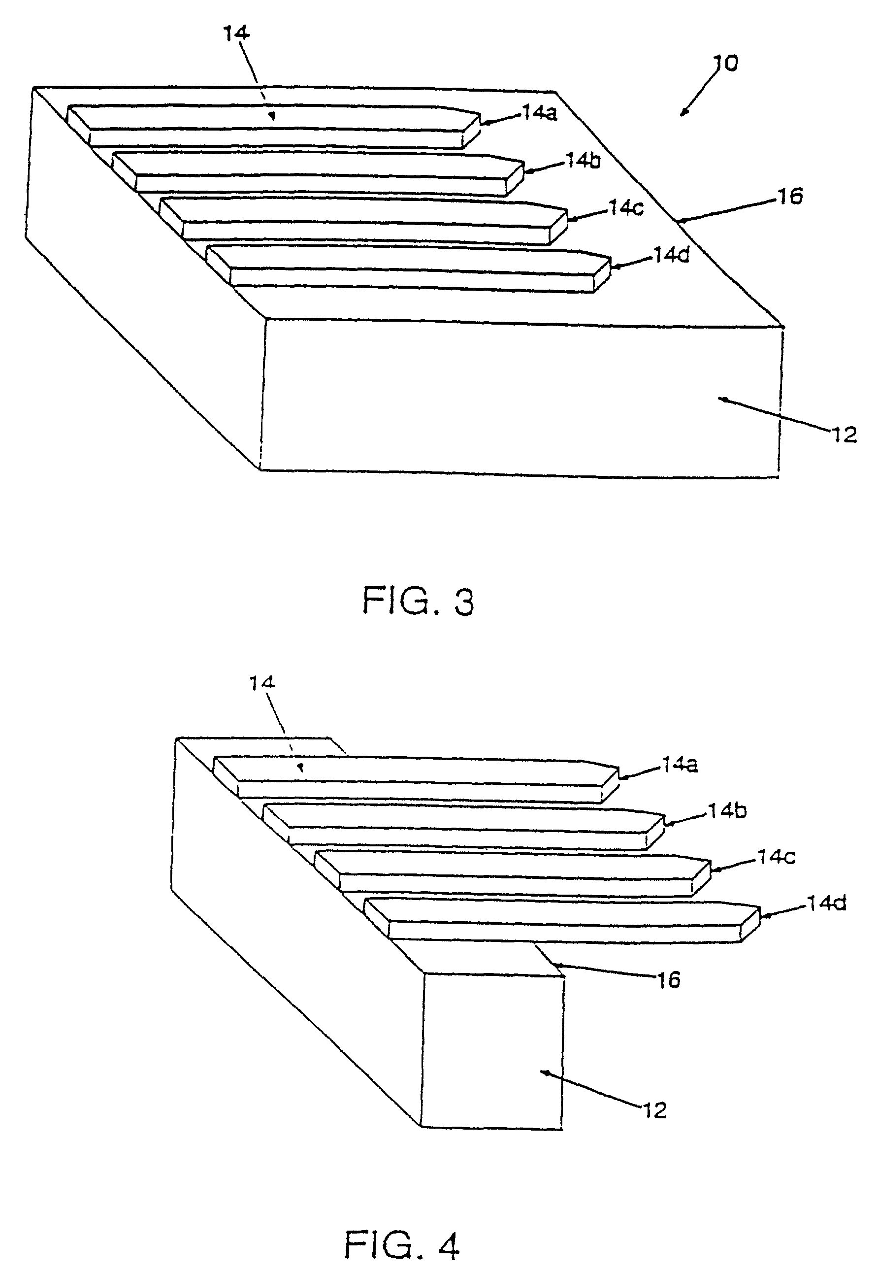
[0018](b) a first multitude of conductive probe arms positioned in co-planar relationship with surface of said supporting body, and freely extending from said supporting body, giving individually flexible motion of said first multitude of conductive probe arms; and
[0019](c) said conducting probe arms originating from a process of producing said multi-point probe including producing said conductive probe arms on supporting wafer body in facial contact with said supporting wafer body and removal of a part of said wafer body providing said supporting body and providing said conductive probe arms freely extending from said supporting body.
[0020]According to the basic realisation of the present invention, the multi-point probe according to the first aspect of the present invention is implemented in accordance with the technique of producing electronic circuits, in particular involving planar techniques as the probe is produced from a supporting body, originating from a wafer body on which a first multitude of conductive probe arms are produced involving deposition, accomplished by any technique known in the art, such as chemical vapour deposition (CVD), plasma enhanced CVD (PECVD), electron cyclotron resonance (ECR) or sputtering, etching or any other production technique, for example high resolution lithographic methods such as electron-beam lithography, atomic force microscopy (AFM) lithography or laser lithography, whereupon a part of the original supporting body is removed through mechanical grinding or etching producing the freely extending conducting probe arms characteristic to the present invention constituting the test pins of multi-point probes according to the first aspect of the present invention.

Problems solved by technology

However, when the electrical field on the movable part changes in such a way that the piezoelectric element contract or elongates quickly, the force on the movable part can exceed the frictional force between the movable part and the substrate, causing the movable part to change its position relative to the substrate with a fraction of a micrometer.
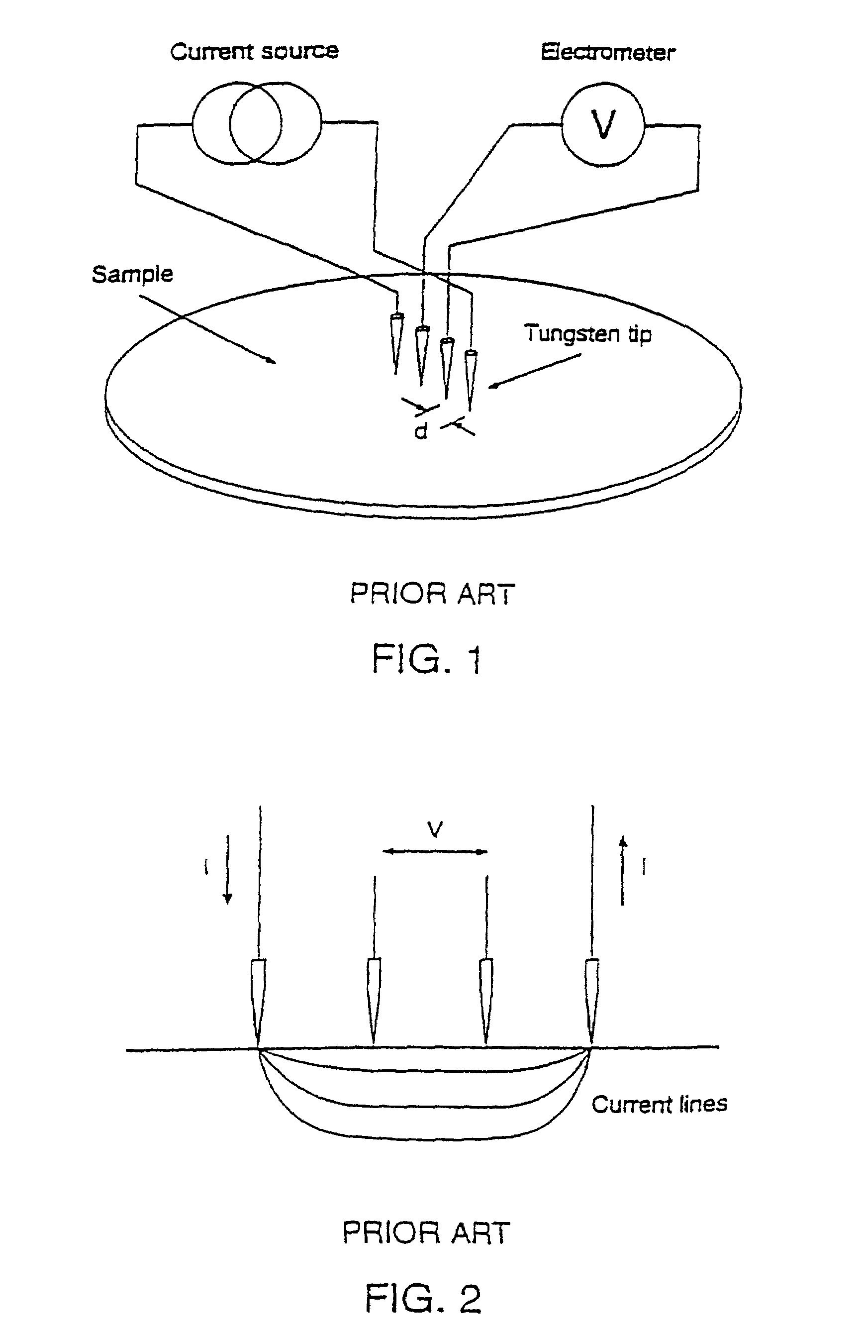
However, since the tips are situated on the same cantilever beam the pressure monitored while monitoring the maximum pressure may possibly leave one tip with an inferior physical contact.
Furthermore, apart from the above described limitations as to establishing contact with the surface of the test sample to be tested the prior art probes possess limitations as to miniaturisation of the testing technique as the probes hitherto known limit the maximum spacing between any two tips to a dimension in the order of 0.5 mm due to the production technique involving mechanical positioning and arresting of the individual testing pins or testing tips, in particular as far as the four-point probes are concerned, and as far as the SR-probes are concerned exhibit extreme complexity as far as the overall structure is concerned and also certain drawbacks as far as the utilisation of the SR-probe due to the overall structure of the SR-probe.

Method used


Image

  • Nano-drive for high resolution positioning and for positioning of a multi-point probe
  • Nano-drive for high resolution positioning and for positioning of a multi-point probe
  • Nano-drive for high resolution positioning and for positioning of a multi-point probe

Examples


second embodiment

[0155]In a second embodiment, the movable member in the cylindrical nano-drive according to the invention is a hollow tube which is closed in one end, as shown in FIG. 18b. The electromechanical actuator is fixed to the bottom of the tube.

third embodiment

[0156]In a third embodiment, the movable member in the cylindrical nano-drive according to the invention is a hollow tube which is closed in one end, and is movably supported on the inside of the tube as shown in FIG. 18c.

[0157]FIG. 19a shows an embodiment of a micro-pipette 1901 according to the invention. The micro-pipette consists of a cylindrical nano-drive according to the invention, which has a movable member 1907 movably supported inside a tube 1903, said tube having an opening 1913 through which very small amounts of liquid or gas can be dispensed or acquired. An electro-mechanical actuator 1909 is fixed to the movable member, and an inertial member 1911 is fixed to the distal end of the actuator. The position of the movable member is controlled by electrical signals applied to the electromechanical actuator in such a way that the volume of gas or liquid in the tube is controlled with very high accuracy. FIG. 19b shows a sectional view of the micro-pipette.

[0158]FIG. 20a sh...


PUM


Abstract

The multi-point probe comprises a supporting body defining a first surface, a first multitude of conductive probe arms each of the probe arms defining a proximal end and a distal end being positioned in co-planar relationship with the first surface of the supporting body. The probe arms are connected to the supporting body at the proximal ends thereof and have the distal ends freely extending from the supporting body, giving individually flexible motion to the first multitude of probe arms. The probe arms originate from a process of producing the probe arms on a wafer body in facial contact with the wafer body and removal of a part of the wafer body providing the supporting body and providing the probe arms freely extending therefrom. The multi-point probe further comprises a third multitude of tip elements extending from the distal end of the first multitude of probe arms. The tip elements originate from a process of metallization of electron beam depositions on the probe arms at the distal ends thereof.

Description

[0001]This application is a continuation of international application Ser. No. PCT / DK00 / 00513, filed 15 Sep. 2000 and a Continuation-In-Part of U.S. application Ser. No. 09 / 750,645, filed on 28 Dec. 2000 now abandoned, which is a continuation of PCT / DK99 / 00391 filed on 8 Jul. 1999.FIELD OF THE INVENTION[0002]The present invention generally relates to a nano-drive for high resolution positioning and for positioning of a multi-point probe and further relates to the technique of testing electric properties on a specific location of a test sample and in particular the technique of probing and analyzing semiconductor integrated circuits for example of LSI and VLSI complexity.DESCRIPTION OF THE RELATED ART[0003]A method for creating very small movements by means of inertial force is known from the literature, for example U.S. Pat. No. 5,229,679. This method will now be described referring to FIG. 17.[0004]An apparatus for creating very small movements according to prior art, comprises a s...

Claims


Application Information

Patent Timeline
IPC IPC(8): G01R1/073G01R1/067G01R27/04G01R27/14G01R31/26G01R31/28
CPCG01R1/073G01R27/14G01R1/07307G01R31/2831G01R31/2648G01R27/04G01R1/06727
Inventor PETERSEN, CHRISTIAN LETHQUAADE, ULRICHNIELSEN, PETER FOLMERGREY, FRANCOISBOGGILD, PETER
Owner CAPRES
Learn More