Laser mask and crystallization method using the same

a laser mask and crystallization method technology, applied in the field of laser mask and crystallization method using the same, can solve the problems of reduced signal distortion, increased picture quality, and use in peripheral circuits, and achieve the effect of improving crystallization characteristics and improving crystallization characteristics

Inactive Publication Date: 2008-01-08
LG DISPLAY CO LTD
View PDF15 Cites 12 Cited by
  • Summary
  • Abstract
  • Description
  • Claims
  • Application Information

AI Technical Summary

Benefits of technology

[0029]An advantage of the present invention is to provide a laser mask and a crystallization method using the same that can improve the crystallization characteristics of silicon thin film.
[0030]Still another advantage of the present invention is to provide a liquid crystal display device including a silicon thin film having improved crystallization characteristics fabricated by the crystallization method described herein.

Problems solved by technology

However, the field effect mobility of the a-Si TFT is about 1 cm2 / Vsec, which prevents its use in peripheral circuits that apply signals to the pixels, because the peripheral circuits generally operate at more than 1 MHz.
More specifically, the increased frequency decreases the charging time of a signal applied to a pixel such that distortion of the signal is decreased and the picture quality increases.
However, there are many defects in the grains.
Although not as bad as grain boundaries in a poly-Si TFT, these defects affect negatively on the performance of a poly-Si TFT.
However, because this crystallization only occurs when the laser energy is such that the solid seeds 35 remain on the interface with the buffer layer 11, the process margin is very limited.
In addition, because the solid seeds 35 are generated non-uniformly the crystallized grains 30A-30C of the polycrystalline silicon thin film have different crystallization directions, thereby resulting in non-uniform crystallization characteristics.
However, the SLS has the following problems.
As a result, the process time for crystallizing a large-size amorphous silicon thin film is lengthened and the process yield becomes low.

Method used


Image

  • Laser mask and crystallization method using the same
  • Laser mask and crystallization method using the same
  • Laser mask and crystallization method using the same

Examples


first embodiment

[0090]A laser mask and a process for crystallizing a large-size silicon thin film using the same according to the present invention will now be described. FIG. 15A illustrates a method for constructing a laser mask according to the present invention.

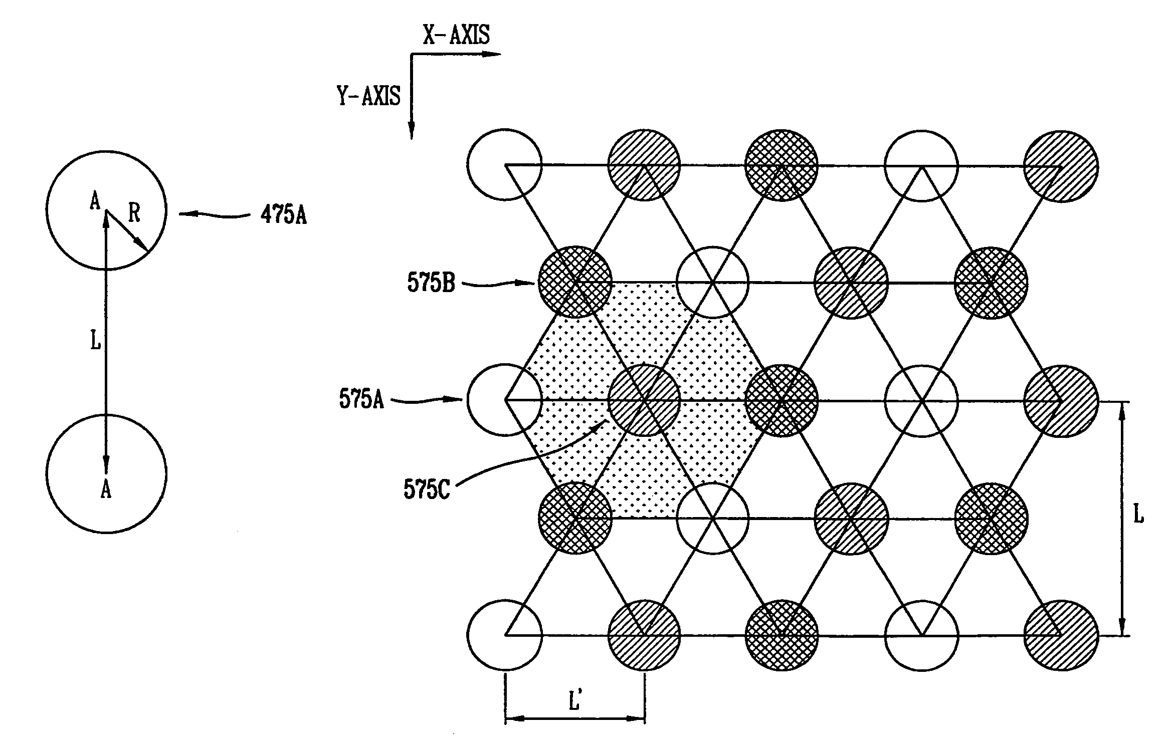
[0091]Referring to FIG. 15A, a mask pattern 675A of the position ‘A’ is formed in a first block 680′ indicated by a square solid line, a mask pattern 675C of the position ‘C’ is formed in a second block 680″, and a mask pattern 675B of the position ‘B’ is formed in a third block 680′″. The three mask patterns 675A to 675C are formed in the three blocks 680′ to 680′″ of the laser mask according to the pattern constructing method of the present invention shown in FIG. 10 or FIG. 12. In the first block 680′, twelve transmitting regions (the mask pattern 675A at the position of ‘A’) having a circular shape are arranged in a 4 columns×3 rows matrix configuration. To be sure, the transmitting regions are arranged crisscross in the odd and even...

second embodiment

[0106]Another example of positioning the three mask patterns will now be described in detail. FIG. 17 illustrates a method for constructing periodic patterns in a laser mask according to the present invention.

[0107]Referring to FIG. 17, in constructing circular transmitting regions (A, B and C) in the laser mask, the laser mask is divided into three blocks to remove a shot mark. A laser transmitting region 775A having the position ‘A’ is formed in a first block, a transmitting region 775B having the position ‘B’ is formed in the second block, and a transmitting region 775C having the position ‘C’ is formed in the third block. That is, as mentioned above, the circular mask patterns 775A to 775C are sequentially formed in each of the three blocks of the laser crystallization mask. In this embodiment, the mask pattern 775B of the position ‘B’ is positioned at the center of the regular hexagon shown in FIG. 17, but the present invention is not limited thereto. The transmitting region 77...


PUM

PropertyMeasurementUnit
driving voltageaaaaaaaaaa
melting pointaaaaaaaaaa

Abstract

A crystallization method using a mask includes providing a substrate having a semiconductor layer; positioning a mask over the substrate, the mask having first, second and third blocks, each block having a periodic pattern including a plurality of transmitting regions and a blocking region, the periodic pattern of the first block having a first position, the periodic pattern of the second block having a second position, the periodic pattern of the third block having a third position, the first, second and third positions being different from each other; and crystallizing the semiconductor layer by irradiating a laser beam through the mask.

Description

[0001]This application claims the benefit of Korean Patent Application No. 2003-99387, filed on Dec. 29, 2003, which is hereby incorporated by reference for all purposes as if fully set forth herein.BACKGROUND OF THE INVENTION[0002]1. Field of the Invention[0003]The present invention relates to a laser mask and a crystallization method using the same, and more particularly, to a laser mask and a crystallization method using the same that can improve the crystallization characteristics of silicon thin film.[0004]2. Discussion of the Related Art[0005]Recently, due to the needs for information displays, especially for portable information displays, thin film type flat panel display (FPD) devices have been actively being researched and commercialized such that the cathode ray tubes (CRT) are being replaced. Of these flat panel display devices, a liquid crystal display (LCD) device displays images using an optical anisotropy of liquid crystal. An LCD device can be used for notebook compu...

Claims


Application Information

Patent Timeline
Patent Type & Authority Patents(United States)
IPC IPC(8): G03F1/00G02F1/1368G02F1/13H01L21/20H01L21/268H01L21/336H01L29/786
CPCB23K26/066H01L21/02488H01L21/02422H01L21/02532H01L21/02595H01L21/0268H01L21/02691G02F1/13
Inventor YOU, JAESUNG
Owner LG DISPLAY CO LTD
Why Eureka
Try Eureka