Method of manufacturing electronic part and electronic part obtained by the method
- Summary
- Abstract
- Description
- Claims
- Application Information
AI Technical Summary
Benefits of technology
Problems solved by technology
Method used
Image
Examples
Example
EXAMPLE 1 AND COMPARATIVE EXAMPLE 1
(1) Preparation of Adhesive Varnish 1
[0107]Into 104 g of methyl ethyl ketone, 106 g of a cresol novolak resin [manufactured by SUMITOMO DUREZ Co., Ltd.; PR-HF-3; the hydroxyl equivalent: 106], 35 g of an epoxy resin of the diallylbisphenol A type [manufactured by NIPPON KAYAKU Co., Ltd.; RE-810NM; the epoxy equivalent: 225] and 210 g an epoxy resin of the dicyclopentadiene type [manufactured by NIPPON KAYAKU Co., LTD.; XD-1000L; the epoxy equivalent: 248] were dissolved and adhesive varnish 1 for metal bonding was prepared.
(2) Preparation of a Multi-Layer Wiring Board
[0108]In an insulation film of a polyimide resin on a flexible substrate for printed wiring [manufactured by SUMITOMO BAKELITE Co., Ltd.; A1FLEC] composed of a copper foil (the metal foil 101; the thickness: 18 μm) and an insulation film of a polyimide resin (the insulation film 102; the thickness: 25 μm), 300 vias (the via 103) each having a diameter of 45 μm at the top and a diameter...
Example
EXAMPLE 2
(1) Preparation of Adhesive Varnish 2
[0117]Into 165 g of methyl ethyl ketone, 106 g of a cresol novolak resin [manufactured by SUMITOMO DUREZ Co., Ltd.; PR-HF-3], 105 g of phenolphthalein [manufactured by TOKYO KASEI Co., Ltd.] and 450 g of an epoxy resin of the diallylbisphenol A type [manufactured by NIPPON KAYAKU Co., Ltd.; RE-810NM] were dissolved and adhesive varnish 2 for metal bonding was prepared.
(2) Preparation of a Multi-Layer Wiring Board
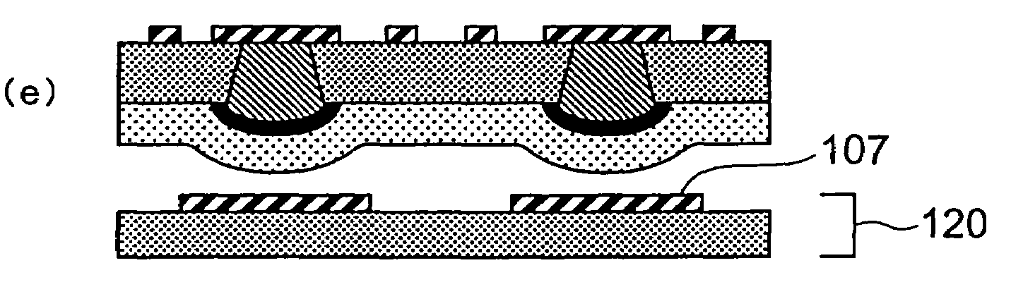
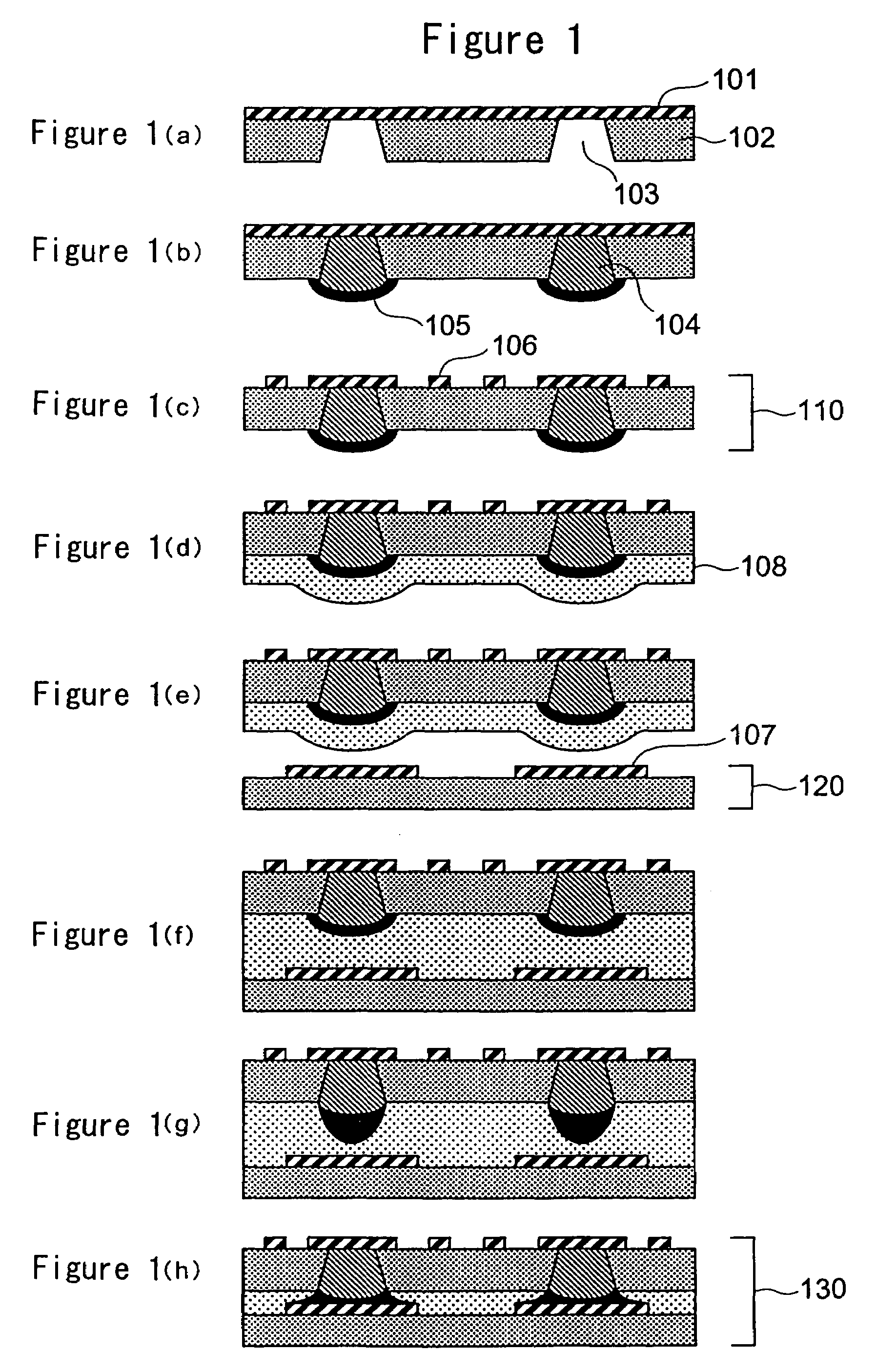
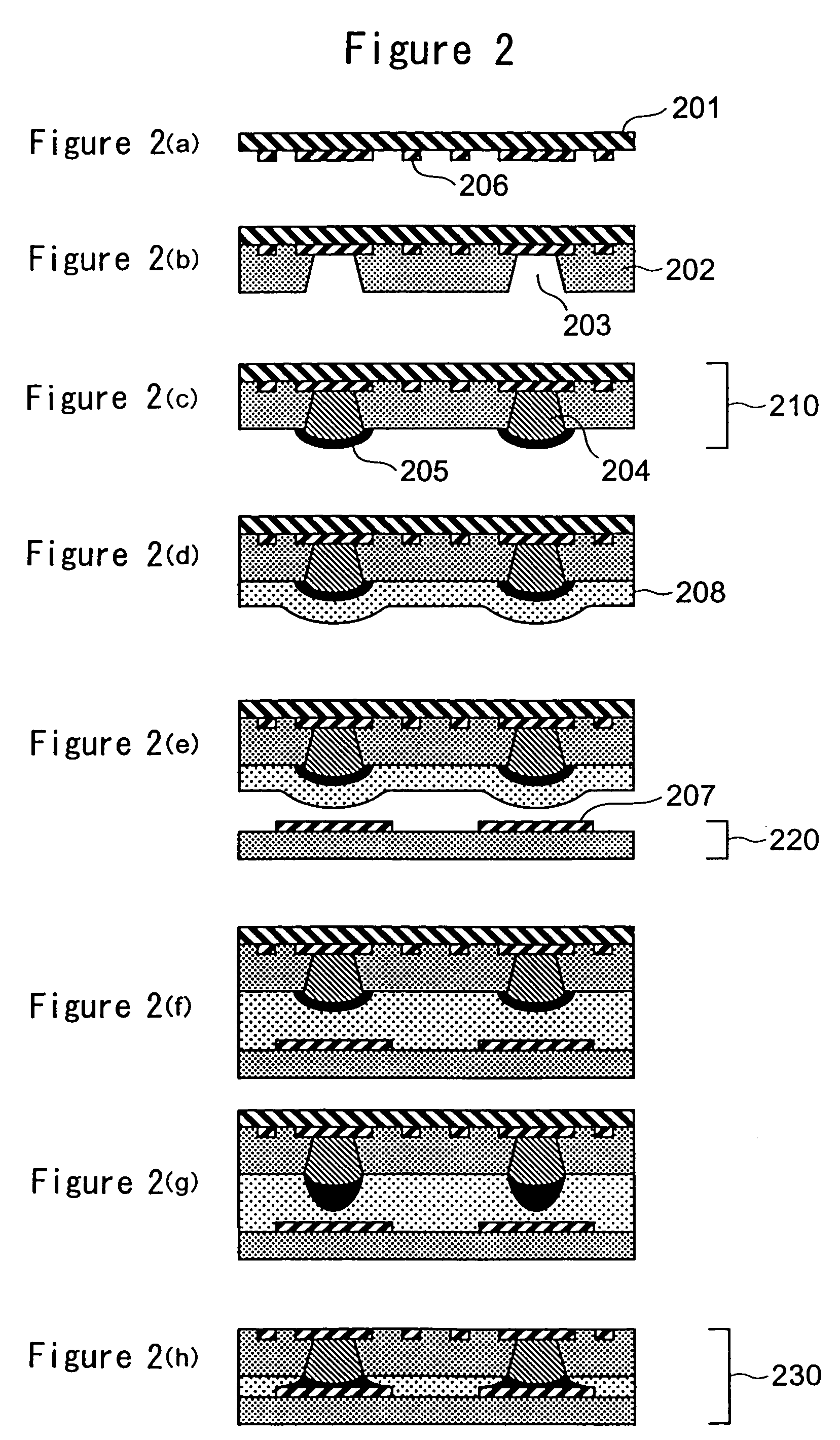
[0118]In an insulation film of a polyimide resin on a flexible substrate for printed wiring (manufactured by SUMITOMO BAKELITE Co., Ltd.; A1FLEC) composed of a copper foil (the metal foil 101; the thickness: 18 μm) and an insulation film of a polyimide resin (the insulation film 102; the thickness: 25 μm), 300 vias (the via 103) each having a diameter of 45 μm at the top and a diameter of 25 μm at the bottom were formed using the UV-YAG laser. After the inside and peripheral portions of the vias were cleaned with an etching liqui...
Example
COMPARATIVE EXAMPLE 2
[0129]The same procedures as those conducted in Example 2 were conducted in steps to the temporary attachment. The obtained temporarily attached sample was heated while the sample was approximately simultaneously pressed. The heating under a pressure was continued to achieve the permanent bonding (condition 4) and a multi-layer wiring board was obtained. The profiles of the temperature and the pressure are shown in FIG. 7.
[0130]The strength of bonding of the soldered portion was measured in accordance with the same method as that in Example 2 and the average shear strength per 1 bump was found to be 275 mN. A section of the bonded portion of the metal was observed in accordance with the same method as that in Example 2 and partial bonding was found.
[0131]The shear strength of the conductor post per one bump was 275 mN in Comparative Example 2 and, in contrast, 402 mN in Example 2. The value in Example 2 was about 1.5 times as great as the value in Comparative Ex...
PUM
Property | Measurement | Unit |
---|---|---|
Fraction | aaaaa | aaaaa |
Percent by mass | aaaaa | aaaaa |
Abstract
Description
Claims
Application Information
- R&D Engineer
- R&D Manager
- IP Professional
- Industry Leading Data Capabilities
- Powerful AI technology
- Patent DNA Extraction
Browse by: Latest US Patents, China's latest patents, Technical Efficacy Thesaurus, Application Domain, Technology Topic.
© 2024 PatSnap. All rights reserved.Legal|Privacy policy|Modern Slavery Act Transparency Statement|Sitemap