Composition which forms an electrically conductive resist layer and a method for patterning a photoresist using the resist layer

a technology of resist layer and resist layer, which is applied in the field of resist layer, can solve the problems of inability to pattern with high resolution and limit the structure resolution, and achieve the effect of dissipating electrical charges and good resolution

Inactive Publication Date: 2008-04-01
POLARIS INNOVATIONS LTD
View PDF16 Cites 1 Cited by
  • Summary
  • Abstract
  • Description
  • Claims
  • Application Information

AI Technical Summary

Benefits of technology

[0008]By crosslinking the composition, it is possible to form an electrically conductive resist layer, which is particularly stable and inert with respect to customary aqueous developer systems of photoresists. At the same time, the electrically conductive resist layer has a sufficiently high conductivity in the range of e.g., 10−4 to 10−1 S / cm2, which enables a very good dissipation of the electrical charges. Moreover, the electrically conductive resist layer can be etched particularly well by means of reactive plasmas, for example an oxygen plasma.
[0010]The resin is advantageously thermally crosslinkable, which is the case for example with so-called self-crosslinking resins. Examples of appropriate self-crosslinking resins are phenol-formaldehyde resins, for example novolak or cresol. These have the advantage that they are also a constituent of conventional chemically amplified photoresists (CA resists), with the result that the electrically conductive resist layer has particularly good chemical compatibility with photoresists that are possibly to be applied on the resist layer.
[0016]The solvent is expediently selected from the solvents methoxypropyl acetate, ethyl lactate, ethyl acetate, cyclohexanone, cyclopentanone, gamma-butyrolactone, hexanol, tetrahydrofuran, methanol and acetontrile. These solvents, and also the mixtures thereof, are particularly well suited to dissolving the resin that can be crosslinked to form a base polymer, the organic compound that can be crosslinked to form an electrically conductive substance, and the crosslinking agent, and thus to creating highly concentrated compositions that are suitably viscous for a coating.
[0017]When a composition according to the invention is crosslinked, in this case not only are covalent bonds linked between individual molecules of the resin or individual molecules of the organic compound that can be crosslinked to form an electrically conductive substance, but also covalent bonds are formed between the base polymer and the electrically conductive organic compound. This has the advantage that an electrically conductive resist layer that is inert particularly well with respect to chemical solvents and is constructed by means of a branched molecular framework is formed during the crosslinking. If the resin is novolak, for example, then the aromatic OH groups can react with further OH groups of novolak oligomers, reactions of the OH group with the aromatic rings of organic compound, e.g. thiophene, also being possible.
[0025]In a further refinement of the method according to the invention, the structures in the photoresist layer may be transferred to the substrate through the resist layer. This may be done for example by means of an oxygen plasma and / or a fluorine-containing plasma. A photomask, for example made of quartz glass, can be used for example as the substrate. It is furthermore possible for a photomask on which a patterned metal layer is at least partly arranged to be used as the substrate. As already mentioned above, in this case the electrically conductive resist layer according to the invention may particularly advantageously enable a particularly good dissipation of charge despite the interruption of the patterned metal layer.
[0026]The composition is advantageously heated for the crosslinking. This makes it possible in a particularly simple manner, in interaction with the crosslinking agent, for the resin and organic compound to be simultaneously interlinked.

Problems solved by technology

The particle size of a layer generally limits the resolution of the structures that can be introduced into the layer.
Many electrically conductive polymers, e.g., polyacetylenes, have very large particle sizes of >0.5 μm, with the result that they cannot be patterned with a high resolution.

Method used


Image

  • Composition which forms an electrically conductive resist layer and a method for patterning a photoresist using the resist layer
  • Composition which forms an electrically conductive resist layer and a method for patterning a photoresist using the resist layer
  • Composition which forms an electrically conductive resist layer and a method for patterning a photoresist using the resist layer

Examples


exemplary embodiment 1

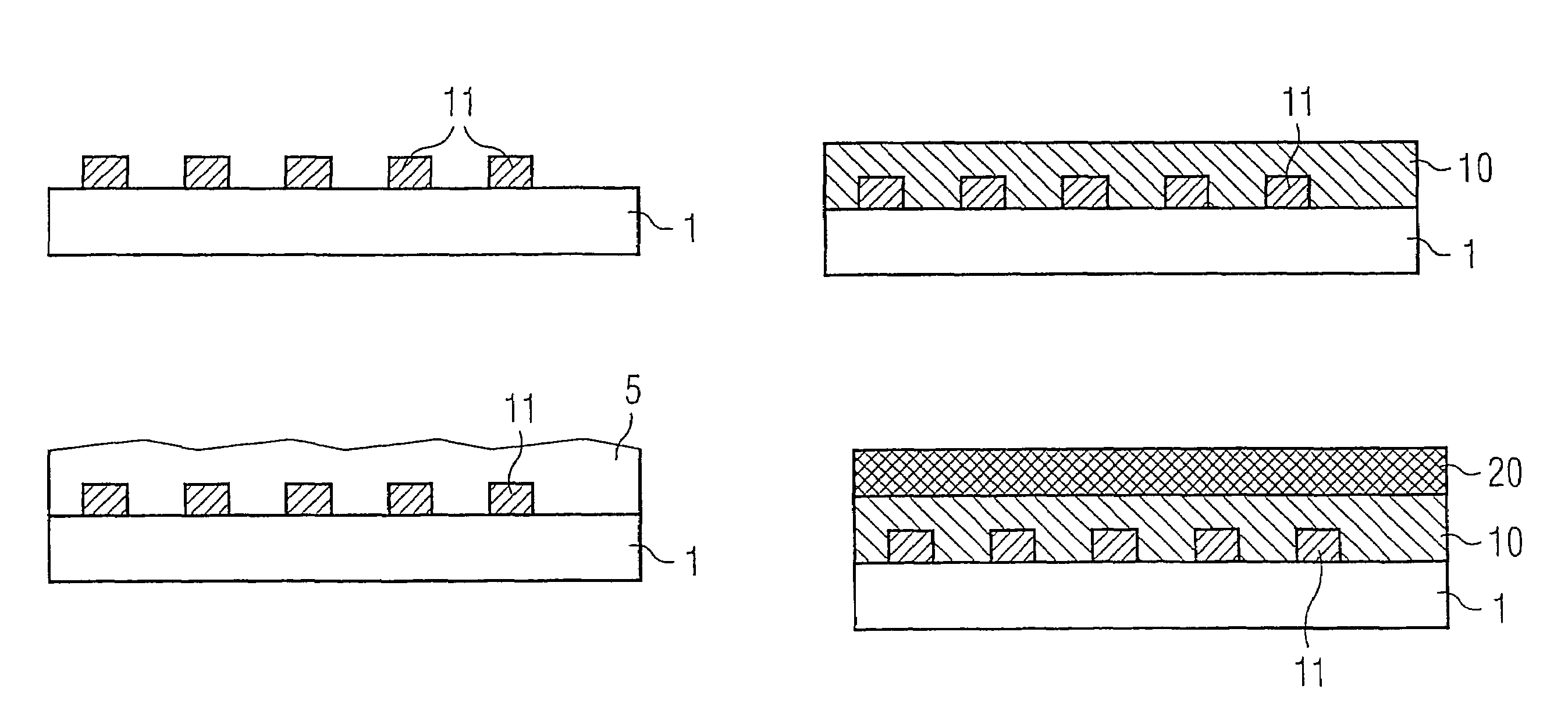
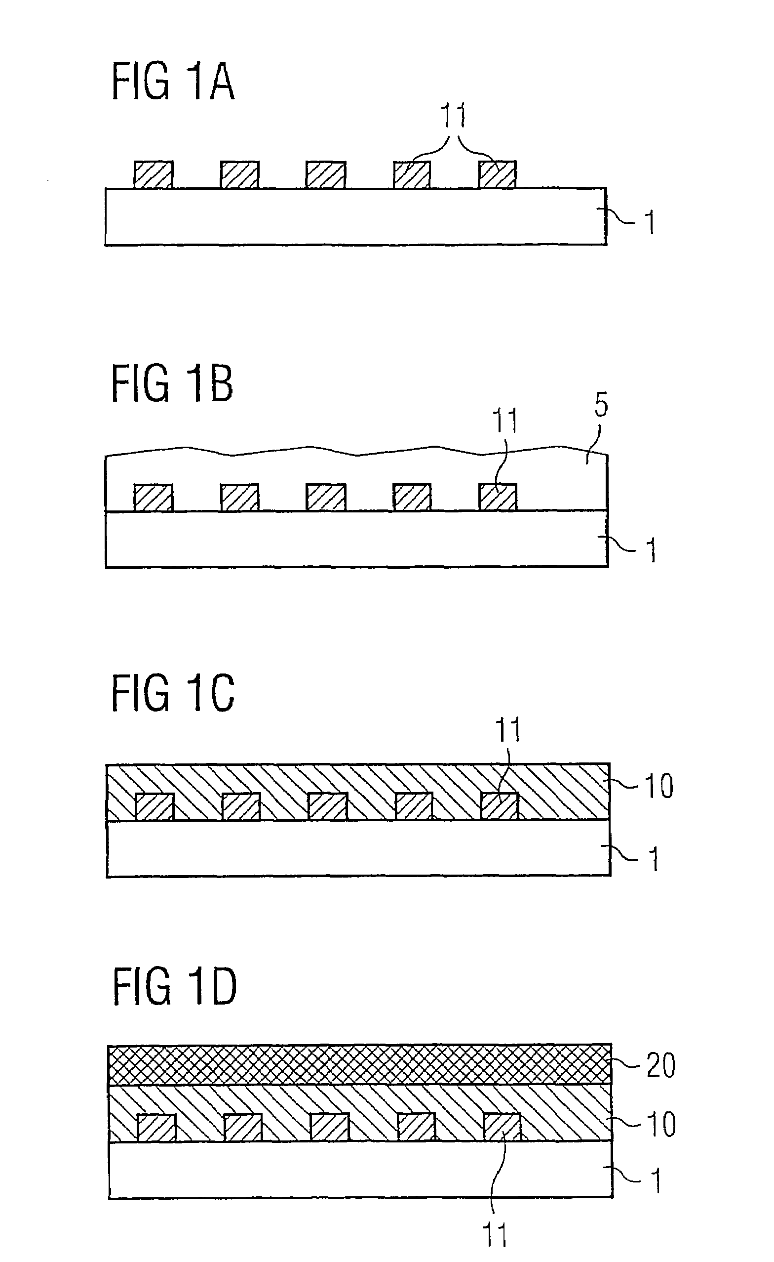
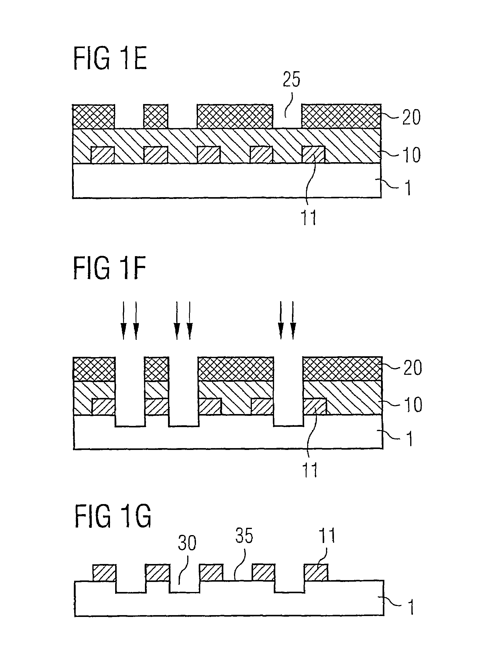
[0038]A composition according to the invention is prepared by admixing 1 g of terthiophene (an organic compound) from the company Aldrich, with 49.5 g of the novolak solution BLC-001 (a resin) from the company Tokyo Ohka and then 49.5 g of a 4-percent strength solution of anhydrous iron(III) chloride in tetrahydrofuran (crossing agent and solvent) are added thereto. The composition obtained is intimately mixed on a shaking device for 30 minutes.

[0039]The composition according to the invention is applied on a 4″ silicon test wafer by means of spincoating (4000 rpm 20 seconds). The electrically conductive resist layer is subsequently formed by crosslinking. For this purpose, the composition is heated at 160° C. for 120 seconds. A large part of the solvent evaporates in the process, resulting in a dry, electrically conductive, dark-gray, transparent resist film having a layer thickness of 0.5 μm on the silicon test wafer.

[0040]The electrically conductive resist layer is subsequently co...

exemplary embodiment 2

[0042]The method is carried out analogously to exemplary embodiment 1; as the composition according to the invention, 1 g of terthiophene is admixed with 49.5 g of novolak solution BLC-001 from Tokyo Ohka and 49.5 g of a 4-percent strength solution of copper perchlorate hexahydrate in tetrahydrofuran are then added.

exemplary embodiment 3

[0043]The method is carried out analogously to exemplary embodiments 1 and 2; as the composition according to the invention, 1 g of terthiophene is admixed with 49.5 g of a cresol-novolak solution from Clariant. Then, 49.5 g of a 4-percent strength solution of copper perchlorate hexahydrate in methoxypropyl acetate are added thereto and the composition obtained is intimately mixed on a shaking device for 30 minutes.


PUM

PropertyMeasurementUnit
particle sizeaaaaaaaaaa
particle sizesaaaaaaaaaa
thicknessaaaaaaaaaa

Abstract

A composition is specified which forms an electrically conductive resist layer and comprises a resin that can be crosslinked to form a base polymer, an organic compound that can be crosslinked to form an electrically conductive substance, a crosslinking agent having an oxidative or reductive action, and at least one solvent. An electrically conductive resist layer of this type may be used for example for dissipating electrical charges when patterning a photoresist by means of electrically charged particles.

Description

[0001]This application is a continuation of co-pending International Application No. PCT / DE03 / 03161, filed Sep. 23, 2003, which designated the United States and was not published in English, and which is based on German Application No. 102 44 197.9, filed Sep. 23, 2002, both of which applications are incorporated herein by reference.TECHNICAL FIELD[0002]The present invention relates generally to resist layers, and more particularly to a composition, which forms an electrically conductive resist layer and a method for patterning a photoresist using the resist layer.BACKGROUND[0003]In semiconductor technology, photoresists situated on a substrate are more and more often being patterned by means of electrically charged particles, for example electrons. In this case, patterning by means of electron beam lithography enables more highly resolved structures than optical lithography techniques. Principally in the fabrication of lithography masks, which generally comprise a quartz glass subs...

Claims


Application Information

Patent Timeline
Patent Type & Authority Patents(United States)
IPC IPC(8): G03F7/00G03F7/004G03F1/00G03F7/038G03F7/09
CPCG03F7/038G03F7/093H01B1/127G03F1/26
Inventor ABARGUES, RAFAELELIAN, KLAUS
Owner POLARIS INNOVATIONS LTD
Why Eureka
Try Eureka