
Semiconductor memory device with increased node capacitance

a node capacitance and memory device technology, applied in semiconductor devices, radio frequency controlled devices, electrical devices, etc., can solve the problems of increasing difficulty in preserving such stored data, correspondingly low node capacitance, and physical size drop of memory cell elements, so as to achieve less insulating

Active Publication Date: 2008-04-01
AURIGA INNOVATIONS INC
View PDF22 Cites 3 Cited by
  • Summary
  • Abstract
  • Description
  • Claims
  • Application Information

AI Technical Summary

Benefits of technology

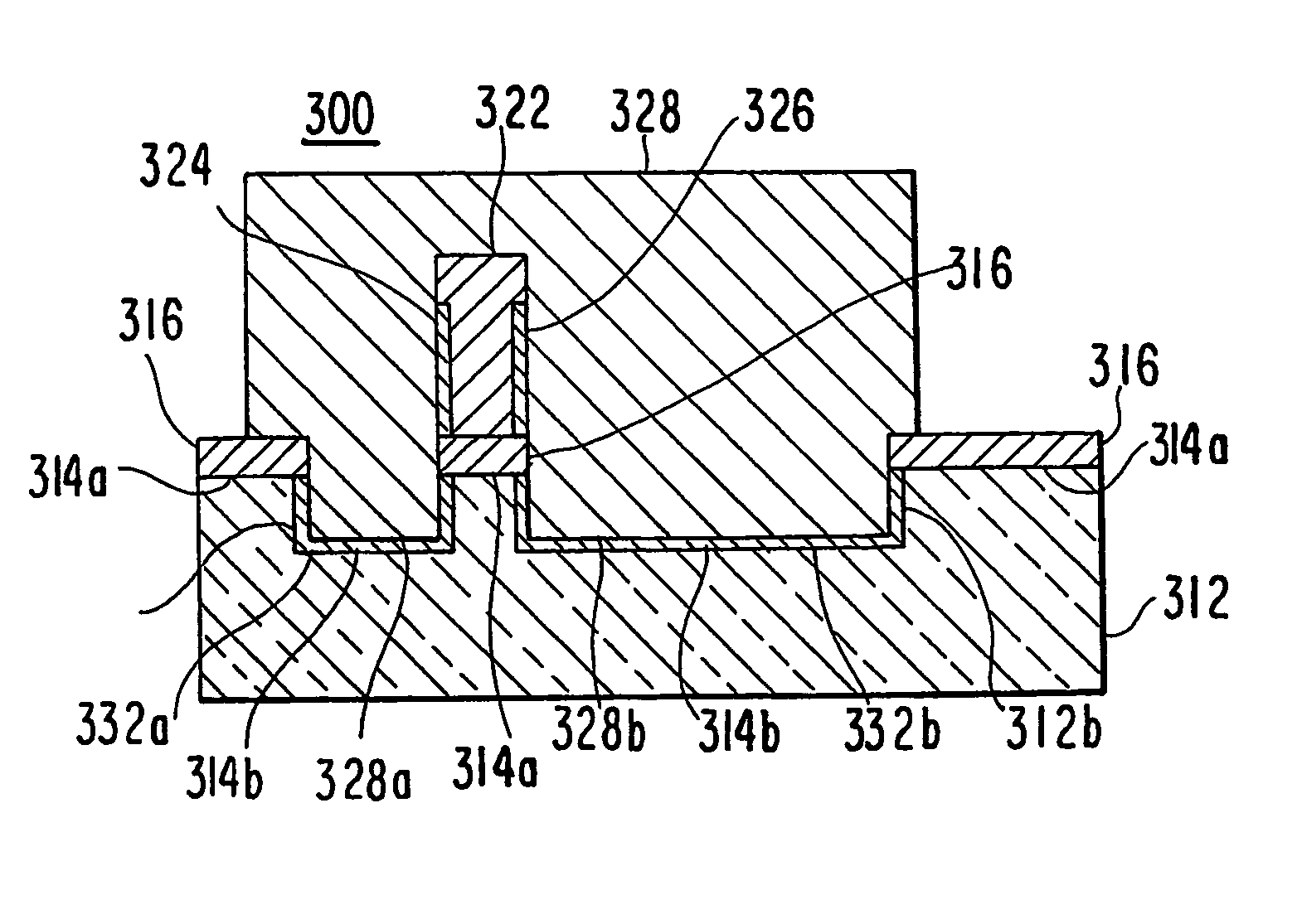
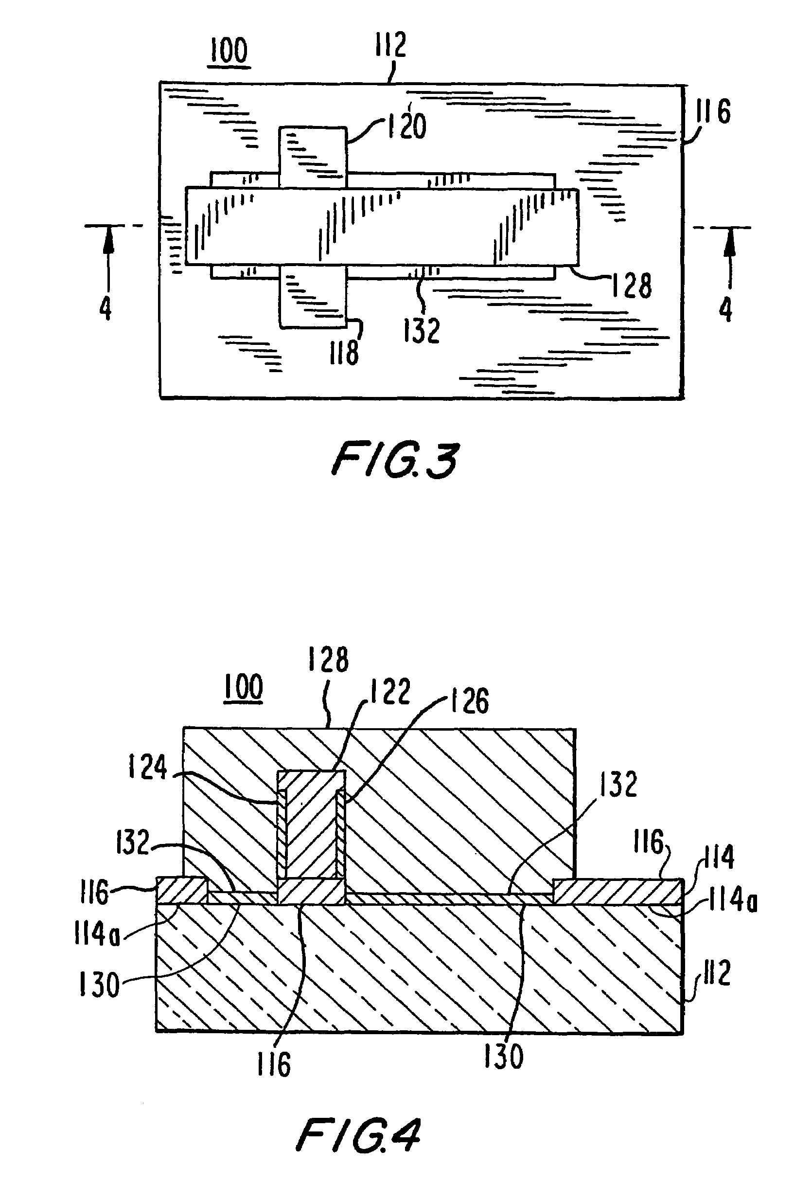
"The present invention provides a semiconductor memory device that avoids difficulties of prior art. It has increased node capacitance to enable a low soft error rate. Additionally, it has increased node capacitance without requiring an increase in area. The device includes a substrate with a first dielectric layer covering a first portion of the substrate, and a second dielectric layer having a different property and at least partly covering the second portion of the substrate. The second dielectric layer provides a greater gate capacitance with respect to the substrate than a gate formed over the first dielectric layer. The device can be an SRAM memory cell, especially a FinFET. The substrate can have an upwardly-facing first surface and an upwardly-facing second surface, and the first and second dielectric layers can be buried oxide layers or thin oxide layers providing less insulating effect. The bulk process can produce a layout where the first dielectric layer is a buried oxide layer and the second dielectric layer is a thin oxide layer providing less insulating effect."

Problems solved by technology

There has been a growing difficulty in preserving such stored data as the scale of integration grows higher and higher and the physical size of the memory cell elements decreases.
This difficulty arises from what are known as soft errors, which are caused primarily by an alpha particle striking one of the memory nodes, or may be caused by circuit noise.
However, as the dimensions of the memory cells are scaled down to fit more devices on the chip, the node capacitances are getting correspondingly very low.
The result is a high susceptibility to circuit noise and radiation, which in turn leads to an unacceptably high soft error rate.

Method used


Image

  • Semiconductor memory device with increased node capacitance
  • Semiconductor memory device with increased node capacitance
  • Semiconductor memory device with increased node capacitance

Examples


Embodiment Construction

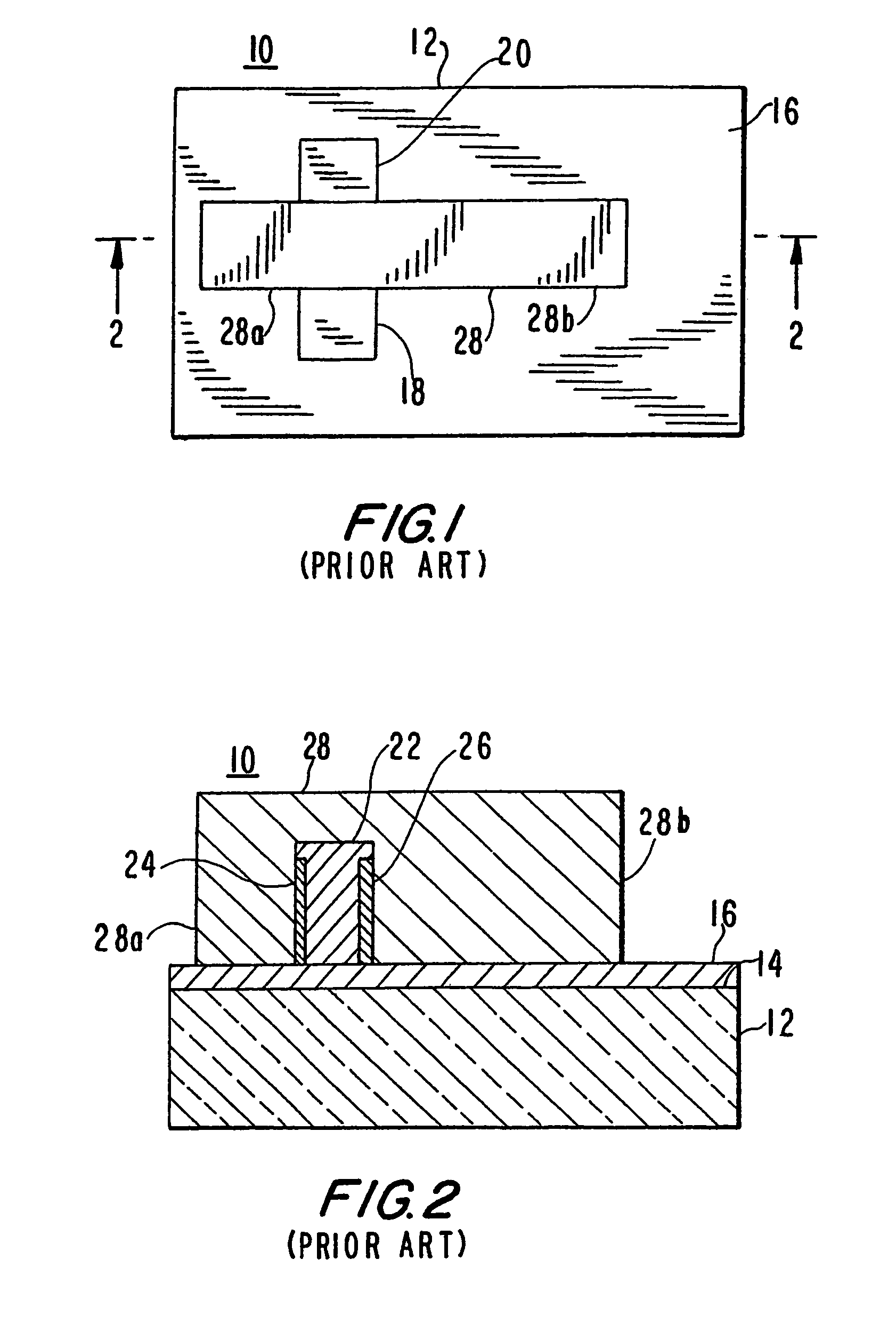
[0025]In the following discussion, the prior art and the embodiments of the present invention will be described in the context of FinFETs. A FinFET is a double-gate MOSFET that is formed by defining and etching a thin, vertical fin in the silicon body of an SOI wafer to connect the source and drain regions. Polysilicon gate electrodes are defined surrounding the fin. In the embodiments discussed below, the double gates are on the right and left sides of the fin and are connected by a portion of the gate passing over the fin. When the FinFET is turned on, the current flow is from source to drain along both the left and right vertical edges of the fin.

[0026]It will be apparent to those of ordinary skill in the art that the following discussion and the accompanying drawings do not reference the complete structure of FinFETs generally or any FinFET in particular, but rather schematically define and compare only those elements of a FinFET useful for explaining the present invention. The ...


PUM


Abstract

An integrated circuit semiconductor memory device having the BOX layer removed from under the gate of a storage transistor to increase the gate-to-substrate capacitance and reduce the soft error rate. The increased node capacitance thus obtained is achieved without requiring a corresponding increase in area.

Description

BACKGROUND ART[0001]This invention relates to an integrated circuit semiconductor memory device such as an SRAM (Static Random Access Memory) or latch that provides increased node capacitance for protection against soft errors.[0002]Semiconductor memory devices such as RAM (random access memory) generally include a number of memory cells each formed of a number of transistors. Generally, two storage transistors are coupled between two pass gate transistors, and a bit line is coupled to each of the pass gate transistors. Each pass gate transistor has a gate electrode coupled to a word line, and an address signal is provided on the word line associated with a particular memory cell in order to select that memory cell and read out the stored data therefrom. With the memory cell so selected, its data is read out from the memory node of the memory cell (or data is written therein) through the pass gate transistors via the bit lines. It is of course important that the data stored in the m...

Claims


Application Information

Patent Timeline
Patent Type & Authority Patents(United States)
IPC IPC(8): H01L29/76H10B10/00H01L21/336H01L27/12H01L27/148H01L29/786
CPCH01L27/11H01L27/1211H01L29/66795H01L29/785H10B10/00H01L21/845
Inventor ANDERSON, BRENT A.BRYANT, ANDRESNOWAK, EDWARD J.
Owner AURIGA INNOVATIONS INC
Learn More