Radiation detecting apparatus and method for manufacturing the same

a technology of radiation detection and detecting apparatus, which is applied in the direction of radiation measurement, measurement devices, instruments, etc., can solve the problems of long vacuum plasma treatment time, inability to reform the surface of the underlayer without damaging the sensor panel, and high current of photoelectric conversion devices, so as to prevent peeling, uniform optical conversion efficiency, and high precision of columnar crystals

Inactive Publication Date: 2008-04-08
CANON KK
View PDF15 Cites 7 Cited by
  • Summary
  • Abstract
  • Description
  • Claims
  • Application Information

AI Technical Summary

Benefits of technology

[0010]Accordingly, an object of the present invention is to provide a high-sensitive, high-definition radiation detecting apparatus exhibiting uniform optical conversion efficiency whose phosphor layer is formed by vapor deposition so as to form uniform, highly precise columnar crystals and is prevented from peeling due to adhesion failure.

Problems solved by technology

First, the phosphor layer may be broken or peeled from an underlayer, a protective layer of the phosphor layer overlying the photoelectric conversion devices, by a heat and humidity test because the adhesion between the phosphor layer and the underlayer is low.
Second, in connection with a corona discharge treatment, which is a common surface treatment for enhancing the adhesion of the underlayer to the phosphor layer, when the corona discharge treatment is applied to the underlayer overlying the photoelectric conversion devices of the sensor panel, current of the photoelectric conversion devices is likely to vary when the TFTs are in an off state, or when a wire of the photoelectric conversion devices is broken. Thus, it has been impossible to reform the surface of the underlayer without damaging the sensor panel.
However, vacuum plasma treatment takes a long time and its process is complicated because it is performed under a high vacuum, and is thus undesirable.

Method used


Image

  • Radiation detecting apparatus and method for manufacturing the same
  • Radiation detecting apparatus and method for manufacturing the same
  • Radiation detecting apparatus and method for manufacturing the same

Examples


first embodiment

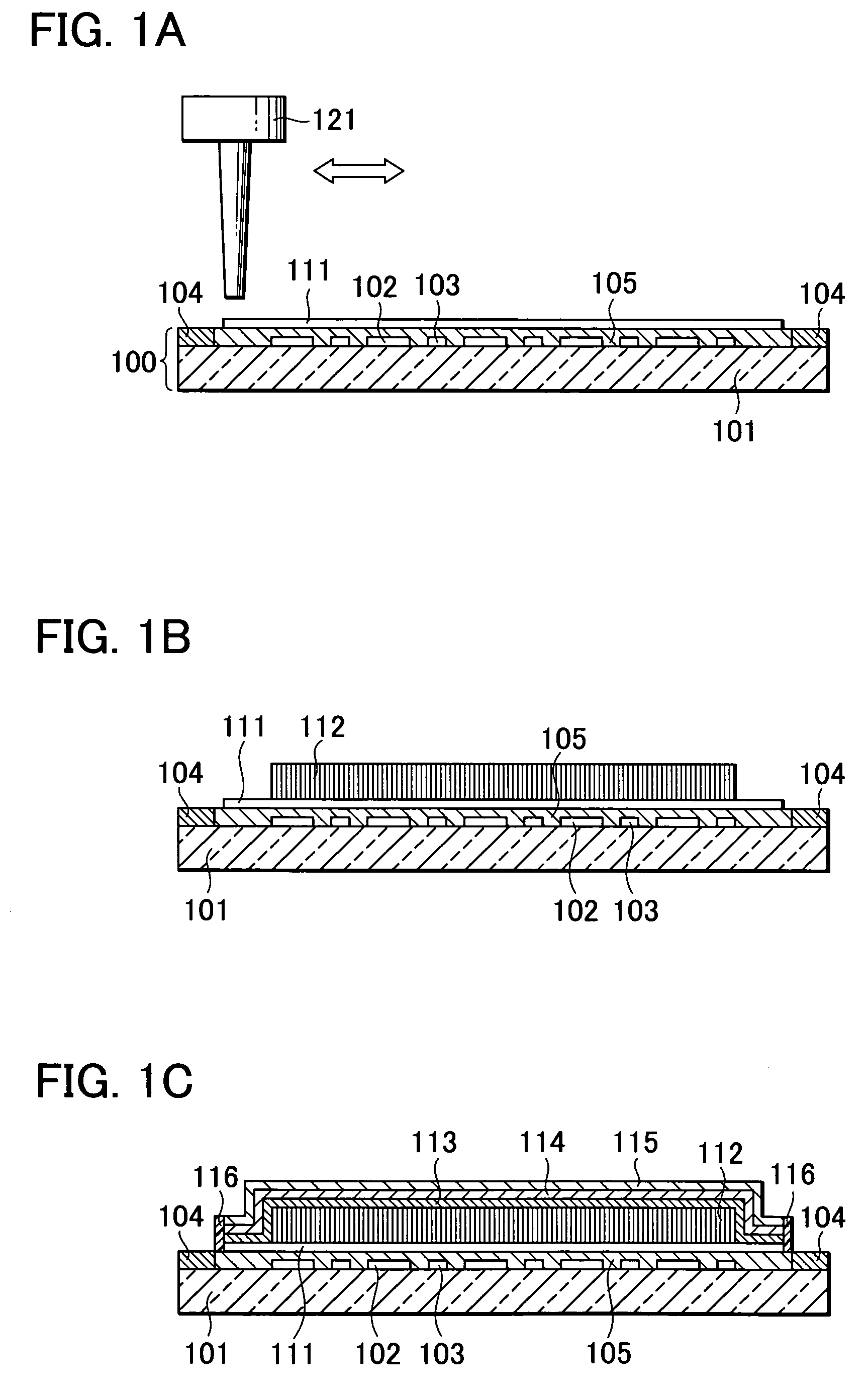
[0025]FIGS. 1A to 1C are sectional views showing the process steps for manufacturing a radiation detecting apparatus according to a first embodiment of the present invention.

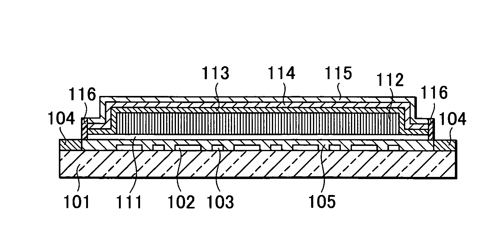
[0026]As shown in FIG. 1A, a sensor panel 100 includes: an insulative glass substrate 101; photoelectric conversion devices 102, each including an amorphous silicon photosensor and a TFT; wires 103; lead-out portions 104; and a passivation layer 105 of, for example, silicon nitride, which is provided to cover the photoelectric conversion devices 102. A resin underlayer 111 of a phosphor layer 112 lies on the sensor panel 100. The underlayer 111 doubles as a protective layer for protecting the stiffness of the photoelectric conversion devices 102. The photoelectric conversion devices 102 are two-dimensionally arranged corresponding to pixels. The passivation layer 105 and the underlayer 111 may be referred to as a first protective layer and a second protective layer, respectively.

[0027]A surface of the underlayer...

second embodiment

[0038]The radiation detecting apparatus of the present invention may include a sensor panel having two-dimensionally arranged photoelectric conversion devices and a scintillator panel that are bonded together. The scintillator panel includes an underlayer of a phosphor layer over a substrate, where the phosphor layer is in contact with the underlayer. The surface of the underlayer contacting the phosphor layer is subjected to atmospheric pressure plasma treatment. The adhesion of the underlayer to the phosphor layer can be enhanced, and the diameter of the columnar crystals in the phosphor layer can be controlled, in the same manner as when the underlayer on the sensor panel is surface-treated.

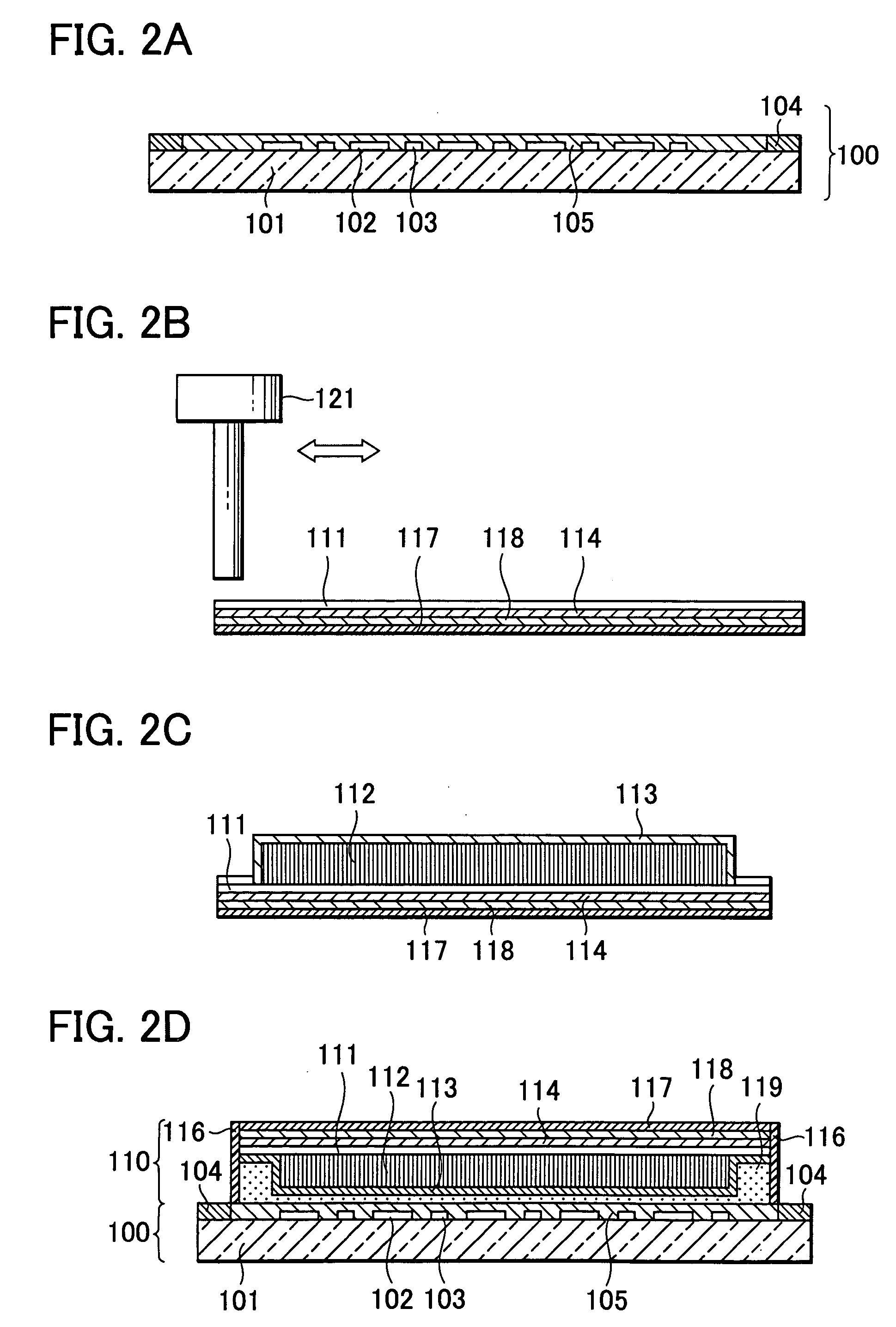
[0039]FIGS. 2A to 2D are sectional views showing process steps for manufacturing a radiation detecting apparatus according to a second embodiment of the present invention.

[0040]FIG. 2A shows a sensor panel 100 of the radiation detecting apparatus. The sensor panel 100 includes an insulative gl...

third embodiment

[0044]FIG. 3 is a representation of a radiodiagnosis system using a radiation detecting apparatus, according to a third embodiment of the present invention.

[0045]X-rays 6060 generated from an x-ray tube 6050 pass through the chest 6062 of a test subject 6061, and enter a radiation detecting apparatus 6040 as shown in FIGS. 2A to 2D. The incoming X-rays include in-vivo information of the subject 6061. The phosphor layer emits light according to the incoming X-rays. The light is converted into electrical signals in the photoelectric conversion devices of the sensor panel and, thus, electrical information is obtained. This information is converted into digital information, and is subsequently processed into an image by an image processor 6070. The image is shown on a display 6080 in a control room.

[0046]The information can be transferred to a remote site through transmitting means, such as a telephone line 6090. Thus, the information can be shown on a display 6081 in a doctor's room ap...


PUM


Abstract

An underlayer of a phosphor layer is disposed on a sensor panel including two-dimensionally arranged photoelectric conversion devices. The surface of the underlayer is subjected to atmospheric pressure plasma treatment. The phosphor layer is formed on the surface-treated underlayer. Then, the phosphor layer is covered with a moisture-resistant protective layer, a reflection layer, and another protective layer. Thus, the phosphor layer is prevented from peeling due to adhesion failure, and is constituted of uniformly shaped crystals by vapor deposition. A resulting radiation detecting apparatus exhibits high sensitivity and high definition, producing a uniform photoelectric conversion efficiency.

Description

BACKGROUND OF THE INVENTION[0001]1. Field of the Invention[0002]The present invention relates to a radiation detecting apparatus for detecting radiation, and in particular, a radiation apparatus used in medical apparatuses, non-destructive examination apparatuses, and the like, and to a method for manufacturing the same. The radiation herein includes α-rays, β-rays, and electromagnetic waves, such as X-rays and γ-rays.[0003]2. Description of the Related Art[0004]In the field of X-ray radiography, X-ray film systems have generally been applied which use a double-coated film and a fluorescent screen containing a phosphor layer. In addition, digital radiation detecting apparatuses have been used because they provide superior image characteristics and allow data to be captured into a networked computer system for sharing.[0005]Among these digital radiation detecting apparatuses are high-sensitive, high-definition apparatuses, as disclosed in U.S. Pat. No. 6,262,422 and U.S. Pat. No. 6,4...

Claims


Application Information

Patent Timeline
Patent Type & Authority Patents(United States)
IPC IPC(8): G01T1/20G01T1/24
CPCG01T1/2018G01T1/2006
Inventor NAGANO, KAZUMI
Owner CANON KK
Why Eureka
Try Eureka