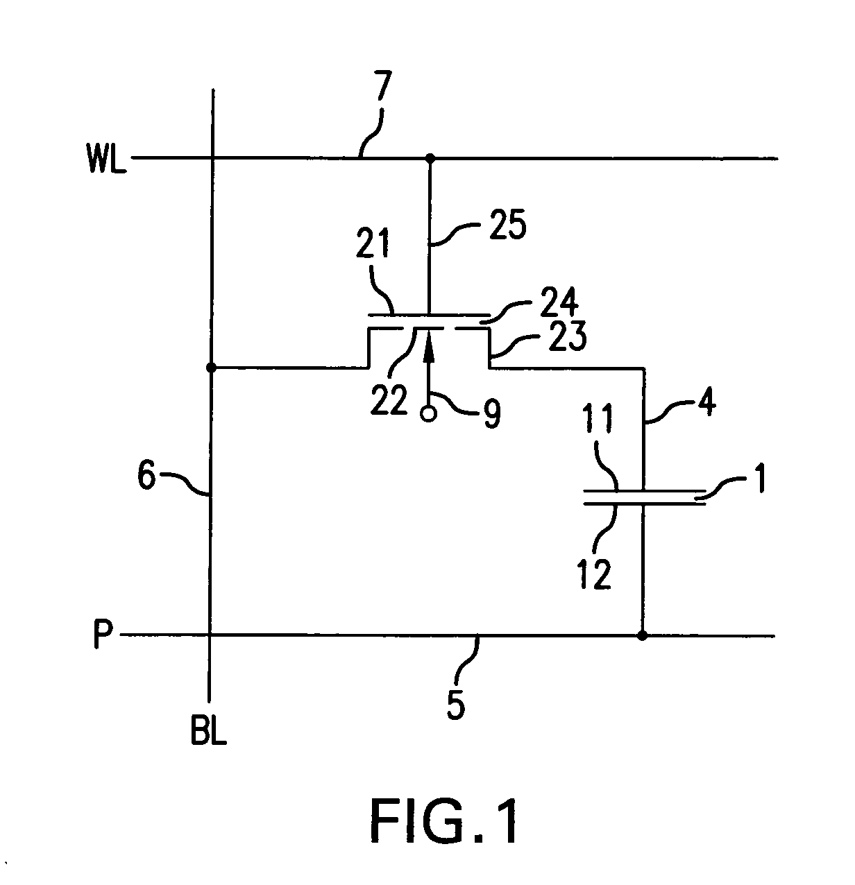
DRAM memory cell

a memory cell and memory technology, applied in the direction of transistors, electrical devices, semiconductor devices, etc., can solve the problems of increasing the width of the planar junction transistor, increasing the leakage current, and increasing the current driver capability of the transistor, so as to achieve good current flow, high carrier mobility, and low doping

Inactive Publication Date: 2008-05-06
POLARIS INNOVATIONS LTD
View PDF8 Cites 28 Cited by
  • Summary
  • Abstract
  • Description
  • Claims
  • Application Information

AI Technical Summary

Benefits of technology

[0010]The present invention provides a DRAM memory cell with a reduced area requirement, the selection transistor formed in planar fashion being distinguished by a high current driver capability and charging of the semiconductor substrate being avoided at the same time.
[0018]It is furthermore preferred, in the case of a DRAM memory cell array, to arrange the DRAM memory cells in matrix-type fashion on the semiconductor substrate, in which case, when using trench capacitors, the trench capacitors are preferably arranged regularly in rows and the trench capacitors of adjacent rows are offset with respect to one another. After the formation of the trench capacitors, which are preferably provided with a buried plate, double gate selection transistors assigned to the trench capacitors are then formed such that firstly a strip-type hard mask layer is produced parallel to the rows of trench capacitors, the hard mask layer strips being arranged essentially between the rows of trench capacitors and the trench capacitors being partly covered. Afterward, spacer layers are produced at the steps of the hard mask layer strips and the uncovered semiconductor surfaces are etched down to a predetermined depth by means of anisotropic etching in the region between the hard mask layer strips and the adjoining spacer layers. The etched-free regions are then in turn filled with spacer layer material, the hard mask layer strips are subsequently removed and the surfaces uncovered under the hard mask layer strips are opened down to the predetermined depth by means of anisotropic etching. Afterward, the spacer layer material is then completely removed and an insulator layer is produced in large-area fashion. After the application of a polysilicon layer and the embodiment of a gate electrode patterning, the source / drain dopings are produced. By virtue of this procedure, DRAM memory cells having trench capacitors and double gate selection transistors can be produced in a simple manner using conventional DRAM process steps.

Problems solved by technology

As the areas of the memory cells become smaller and smaller on account of increasing miniaturization, retaining the current driver capability of the transistor poses an increasing problem.
However, the shrinking of the cell areas and the resultant shrinking of the transistor dimensions mean that the transistor width of the planar junction transistors decreases.
However, there is the problem of increased leakage currents when the gate oxide thickness is reduced or the doping concentrations are higher.
However, vertically embodied transistors are very complicated in terms of process engineering and can be fabricated only with difficulty, in particular with regard to the connection technique of the source / drain regions and of the gate electrodes of the transistor.
What is more, there is the problem that, during the operations of switching the selection transistor on and off, the semiconductor substrate is also concomitantly charged at the same time, and the so-called floating body effect occurs, as a result of which the switching speed of the transistor is greatly impaired.
In the case of vertical selection transistors, however, there is the problem that even with the aid of such substrate connections, the semiconductor substrate can often be discharged only to an inadequate extent.
This configuration has the disadvantage that when the double gate transistor is intended to be used as a selection transistor for a DRAM cell, the silicon layer is charged as a result of the transistor being switched on and off, which significantly impairs the switching speed of the transistor.
Although it is possible to avoid such charging of the silicon layer with the Fin-FET by means of an additional electrical connection, said additional connection can be effected only directly via the silicon surface, which results in an increased area requirement on account of the additional connection area, which is at odds with the desired miniaturization of the DRAM memory cell.

Method used


Image

  • DRAM memory cell
  • DRAM memory cell
  • DRAM memory cell

Examples


second embodiment

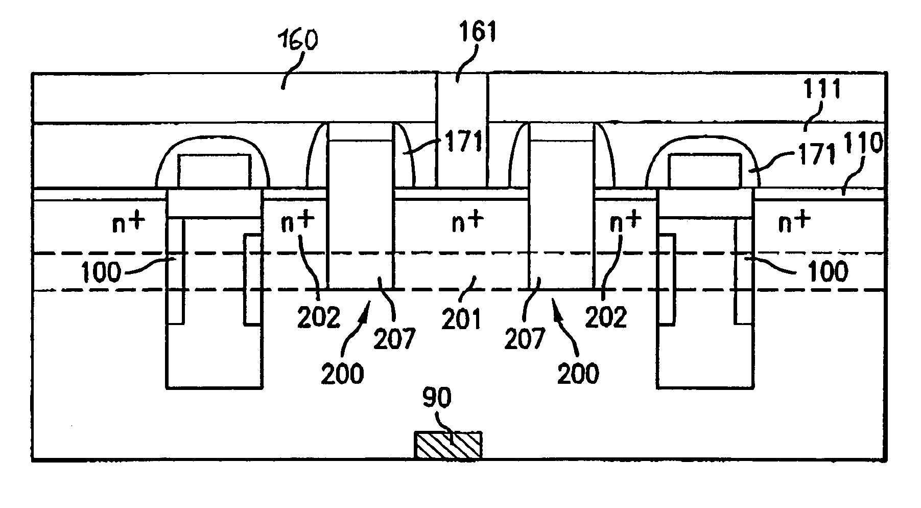
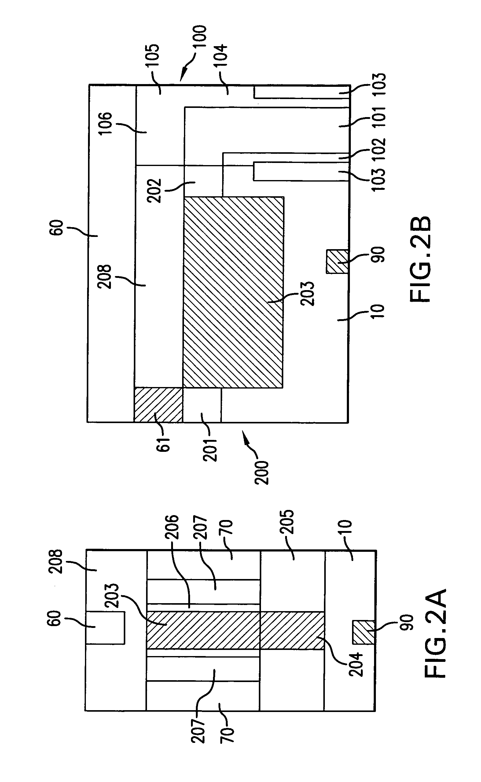
[0043]FIG. 3 shows a DRAM memory cell according to the invention with a double gate transistor. In this embodiment, as shown in particular by the longitudinal section in FIG. 3B, the storage capacitor 300 is formed as a stacked capacitor arranged essentially over a selection transistor 400. In this case, the stacked capacitor 300 has an inner capacitor electrode 301 at the semiconductor surface 10, which electrode has, in cross section, essentially the form of a crown (only partly shown) and preferably comprises a highly n-doped polysilicon layer. The inner capacitor electrode 301 is enclosed by a dielectric layer 302, which is in turn bordered by an outer capacitor electrode 303 (only partly shown) preferably embodied in block-type fashion, which outer capacitor electrode is formed as a highly n-doped polysilicon layer. The inner capacitor electrode 301 is connected via a contact block 304, preferably a highly n-doped polysilicon layer, to a second source / drain electrode 402 of the...

first embodiment

[0048]By means of suitable doping profiles of the channel region of the double gate field-effect transistor according to the invention, it is furthermore possible to improve the current driver capability and also its switching behavior. FIG. 4A shows a cross section through a transistor structure which essentially corresponds to the first embodiment shown in FIG. 2 with a web-like channel region 500 on the semiconductor substrate, which is laterally enclosed in a lower region 504 by an insulator layer 502 adjoined by a thin gate oxide layer 503, which separate lateral gate electrode sections 507 from an upper channel region 501. In this case, the channel region has a channel width W and a channel height Z, corresponding to the height of the gate electrode section 507.

[0049]FIG. 4B shows, on a logarithmic scale, input characteristic curves on such a Fin-FET in the case of a channel length L of 50 nm and a channel width W of 20 nm. In this case, the source / drain electrodes are arsenic...


PUM


Abstract

A DRAM memory cell is provided with a selection transistor, which is arranged horizontally at a semiconductor substrate surface and has a first source / drain electrode, a second source / drain electrode, a channel layer arranged between the first and the second source / drain electrode in the semiconductor substrate, and a gate electrode, which is arranged along the channel layer and is electrically insulated from the channel layer, a storage capacitor, which has a first capacitor electrode and a second capacitor electrode, insulated from the first capacitor electrode, one of the capacitor electrodes of the storage capacitor being electrically conductively connected to one of the source / drain electrodes of the selection transistor, and a semiconductor substrate electrode on the rear side, the gate electrode enclosing the channel layer at at least two opposite sides.

Description

CLAIM FOR PRIORITY[0001]This application claims the benefit of priority to German Application No. 103 20 239.0, filed in the German language on May 7, 2003, the contents of which are hereby incorporated by reference.TECHNICAL FIELD OF THE INVENTION[0002]The invention relates to a DRAM memory cell having a planar selection transistor and a storage capacitor connected to the planar selection transistor.BACKGROUND OF THE INVENTION[0003]In order to obtain a sufficiently large read signal of the DRAM memory cell, the storage capacitor has to provide a sufficient storage capacitance. On account of the limited memory cell area, storage capacitors which utilize the third dimension are therefore used. One embodiment of such a three-dimensional storage capacitor is a so-called trench capacitor, which is arranged in a manner laterally adjoining the selection transistor, preferably essentially below the selection transistor, the inner capacitor electrode arranged in a trench being electrically ...

Claims


Application Information

Patent Timeline
Patent Type & Authority Patents(United States)
IPC IPC(8): H01L27/108H01L29/12H01L31/112H01L21/8238H01L21/8242
CPCH01L27/10823H01L27/10826H01L27/10891H01L27/10808H01L27/10829H01L29/7851H10B12/31H10B12/34H10B12/36H10B12/37H10B12/488
Inventor LUYKEN, RICHARD J.HOFMANN, FRANZRISCH, LOTHARMANGER, DIRKROSNER, WOLFGANGSCHLOSSER, TILLSPECHT, MICHAEL
Owner POLARIS INNOVATIONS LTD
Why Eureka
Try Eureka