Methods and configurations for manufacturing hinges for micro-mirror devices

a technology of micro-mirrors and hinges, applied in the direction of optics, instruments, optical elements, etc., can solve the problems of mechanical fatigue and creep phenomena of metal hinges commonly implemented in commercially available micro-mirrors, limit the practical usefulness of micro-mirrors, and the inability to eliminate metal wires, etc., to facilitate the fabrication of optically flat mirrors, improve elasticity, and simplify the manufacturing process

Active Publication Date: 2008-05-20
IGNITE INC
View PDF2 Cites 6 Cited by
  • Summary
  • Abstract
  • Description
  • Claims
  • Application Information

AI Technical Summary

Benefits of technology

[0019]Many of the advantages of the present invention are due to the material of which the hinge is composed. A doped semiconductor hinge offers a conductive means by which the micro-mirror can be biased while improving elasticity and simplifying the manufacturing process. In addition the material is robust under extreme temperatures and immune to the memory hinge effects caused by creep. Furthermore, the hinge architecture according to the present invention facilitates the fabrication of an optically flat mirror and hidden hinge further simplifies the manufacturing process by allowing a direct connection to the micro-mirror.
[0020]The present invention further provides new and improved processes for fabricating the micromirrors and the control circuits with the metal wires for transmitting control signals. The improved processes allow for high temperature process to crystallize and strengthen the doped semiconductor hinges without damaging the metal wire and metal connections to the transistors such that more reliable semiconductor hinges can be formed while avoiding damages to the metal layers.

Problems solved by technology

Even though there are significant advances made in recent years on the technologies of implementing electromechanical micromirror devices as spatial light modulator, there are still limitations and difficulties of practical usefulness of the micromirrors due to the reliability problems caused by the limited life time of the micromirror hinges employed to support the micromirrors.
Specifically, the metal hinges commonly implemented in the commercially available micromirrors tend to have mechanical fatigue and creep phenomena especially when operated in an elevated temperature.
Metal wires cannot be eliminated because they are necessary to control MOS drivers under mirrors and hinges.
Once metal lines are formed, high temperature processes applied to the wafers are not permissible due to the concerns that the metal lines will melt or damaged at elevated temperatures.
A temperature higher than 400 Celsius applied to the wafer is likely to cause damages to the aluminum wires.
Aluminum will be damaged over 400 degree C.
Conversely, high temperature processes are often required to strengthen the hinges made of a semiconductor.
For these reasons, the difficulties of unreliable metal hinges that often encountered in the conventional micromirror device cannot be easily resolved.
The relaxation of the hinge results in a residual tilt when all voltages are removed.
In addition, while duty-cycle contributes to creep, the dominant factor for hinge memory lifetime is temperature.
The address voltage applied, however, requires enough operating margin to compensate for the residual tilt resulting in further design complexity.
The hinge, however, is composed of an aluminum alloy that is highly susceptible to metal creep.
The edges of the spacervia diffract the incident light into the projection system optics when the mirrors are tilted to the off state, thus limiting the pixel architecture's improvement to contrast ratio.
However, this process cannot produce an optically flat mirror since the underlying spacer layer is not flat.
While this reduces the hinge memory by providing a more elastic hinge, it does not eliminate it.
Furthermore, the formation of the multi-layer hinge results in a more complicated manufacturing process as compared to a hinge made of a single material.
These and other prior art utilizing doped semiconductors for their hinge material fail to provide a device architecture in which the hinge is hidden from incoming light.
This is an important disadvantage which results in poor contrast and fill-factor in applications such as image projection.

Method used


Image

  • Methods and configurations for manufacturing hinges for micro-mirror devices
  • Methods and configurations for manufacturing hinges for micro-mirror devices
  • Methods and configurations for manufacturing hinges for micro-mirror devices

Examples


Embodiment Construction

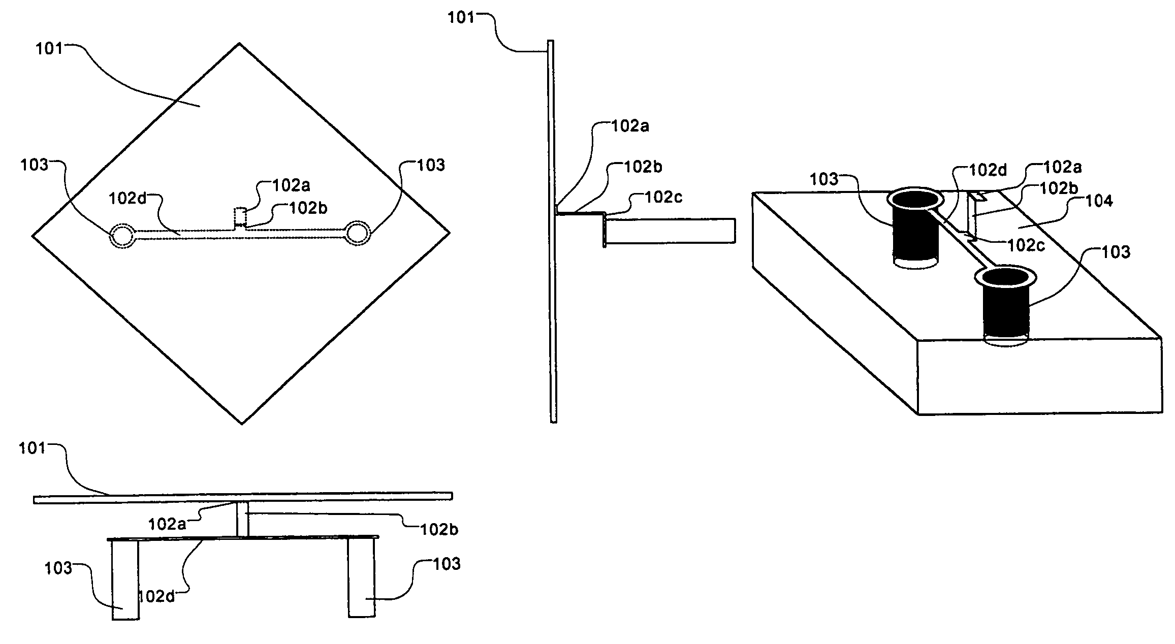
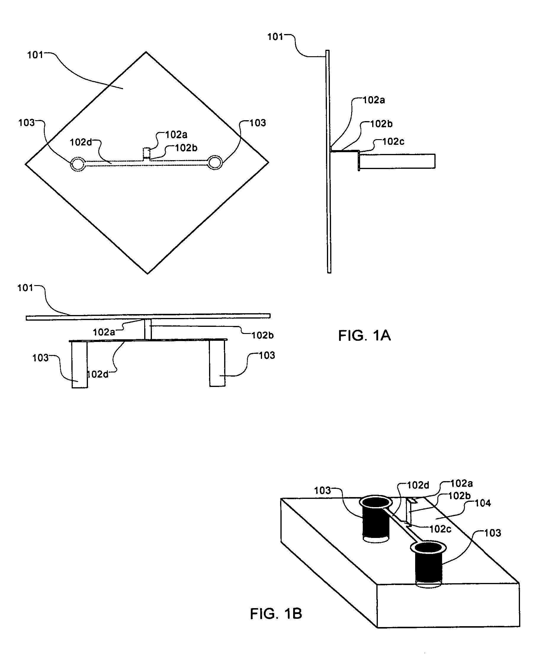
[0032]FIG. 1A shows top and side views of the hinge according to the present invention in the preferred embodiment. In this figure, hinge 102, best described as a compound torsion vertical cantilever, is composed of segments 102a, 102b, 102c and 102d. Segment 102a extends out parallel to the substrate surface and is connected directly to the surface of micro-mirror 101 opposite the substrate. Segment 102b extends out perpendicular to the substrate surface and is connected to segment 102a. The other end of segment 102b is connected to an extension (102c) of segment 102d. Segment 102d is itself a direct extension of support posts 103. Support posts 103 extend below the surface of the substrate (104) and anchor the compound hinge structure (102) to the substrate (104). The thickness of hinge 102 is small relative to the micro-mirror in order to ensure most of the bending occurs at the hinge. This improves the flatness of the micro-mirror in its deflected state. FIG. 1B shows a perspect...


PUM

PropertyMeasurementUnit
temperatureaaaaaaaaaa
annealing temperatureaaaaaaaaaa
diameteraaaaaaaaaa

Abstract

An image display system includes an improved hinge for a micro-mirror device composed of a conductive doped semiconductor and immune to plastic deformation at typical to extreme temperatures. The hinge is directly connected to the micro-mirror device and facilitates the manufacturing of an optically flat micro-mirror. This eliminates Fraunhofer diffraction due to recesses on the reflective surface of the micro-mirror. In addition, the hinge is hidden from incoming light thus improving contrast and fill-factor. The image display system further includes signal transmission metal traces formed on areas between the doped semiconductor hinges. The signal transmission metal traces are formed either before or after a high temperature crystallization process is applied to the hinges.

Description

[0001]This application is a Continuation in Part (CIP) Application of pending U.S. patent application Ser. No. 10 / 698,620 filed on Nov. 1, 2003, now abandoned, and Ser. No. 10 / 918,677 filed on Aug. 14, 2004, now U.S. Pat. No. 7,183,618, by the Applicant of this patent applications. The disclosures made in these patent applications are hereby incorporated by reference in this patent application.TECHNICAL FIELD[0002]This invention relates to micromirror arrays and control circuits to control the micromirrors. More particularly, this invention relates to micromirror array and methods for manufacturing a plurality of micromirrors wherein each micromirror has a reflecting mirror supported on a doped semiconductor hinge.BACKGROUND ART[0003]Even though there are significant advances made in recent years on the technologies of implementing electromechanical micromirror devices as spatial light modulator, there are still limitations and difficulties of practical usefulness of the micromirror...

Claims


Application Information

Patent Timeline
Patent Type & Authority Patents(United States)
IPC IPC(8): G02B26/00G02B26/08G02F1/29
CPCG02B26/0841
Inventor ISHII, FUSAO
Owner IGNITE INC
Why Eureka
Try Eureka