Device fabrication by anisotropic wet etch

a technology of anisotropic wet etching and device fabrication, which is applied in the direction of basic electric elements, semiconductor devices, electrical apparatus, etc., can solve the problems of increasing the complexity of the technology, the difficulty of maintaining performance improvement of devices of deeply submicron generation, and the seriousness of various device effects, so as to reduce the source/drain capacitance, reduce the cross section, and reduce the effect of source/drain capacitan

Inactive Publication Date: 2008-08-12
INT BUSINESS MASCH CORP
View PDF8 Cites 51 Cited by
  • Summary
  • Abstract
  • Description
  • Claims
  • Application Information

AI Technical Summary

Benefits of technology

[0005]In view of the discussed problems, this invention discloses a method of fabrication and a field effect device structure that reduces source / drain capacitance and also allows for device body contact. The method includes the production of a Si based material pedestal, typically by forming a trench in a monocrystalline Si based material member. The top surface and the sidewalls of this pedestal are oriented in a way to be substantially parallel with selected crystallographic planes of the Si based material member. The method further includes the wet etching of the Si based material pedestal with a solution containing ammonium hydroxide (NH4OH). Due to the differing etch rates of the Si based material crystallographic planes in the NH4OH solution, the sidewalls become faceted thereby undercutting a first segment of the Si based material pedestal and creating a second segment underneath the first segment. The second segment has a smaller cross section than the first segment. In the second segment the dopant concentration is sufficiently high for electrical conductivity, thereby allowing a body contact between the Si based material member and the field effect device hosted by the first segment of the Si based material pedestal. The field effect device has its source / drain capacitance lowered because the undercutting of the first segment makes the source / drain of the device similar to those of SOI devices.

Problems solved by technology

As FET (Field Effect Transistor) devices are being scaled down, the technology becomes more complex, and changes in device structures and new fabrication methods are needed to maintain the expected performance enhancement from one generation of devices to the next.
There is great difficulty in maintaining performance improvements in devices of deeply submicron generations.
Various detrimental device effects become more serious with successively decreasing device dimensions.
For instance, with shortening gate lengths the so called short channel effects, most notably the “drain induced barrier lowering” pose severe roadblocks to miniaturization.
In such a case the threshold voltage, Vt, control of the device is more difficult.
Field effect devices built on a bulk Si substrate can have body contact, but suffer from higher source / drain capacitance.

Method used


Image

  • Device fabrication by anisotropic wet etch
  • Device fabrication by anisotropic wet etch
  • Device fabrication by anisotropic wet etch

Examples


Embodiment Construction

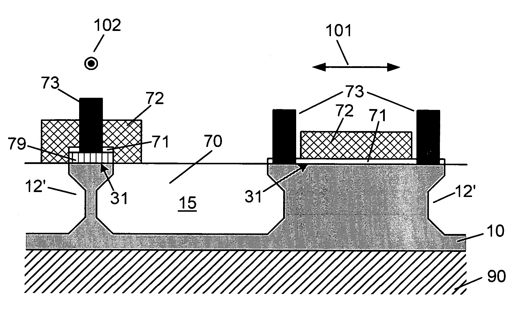
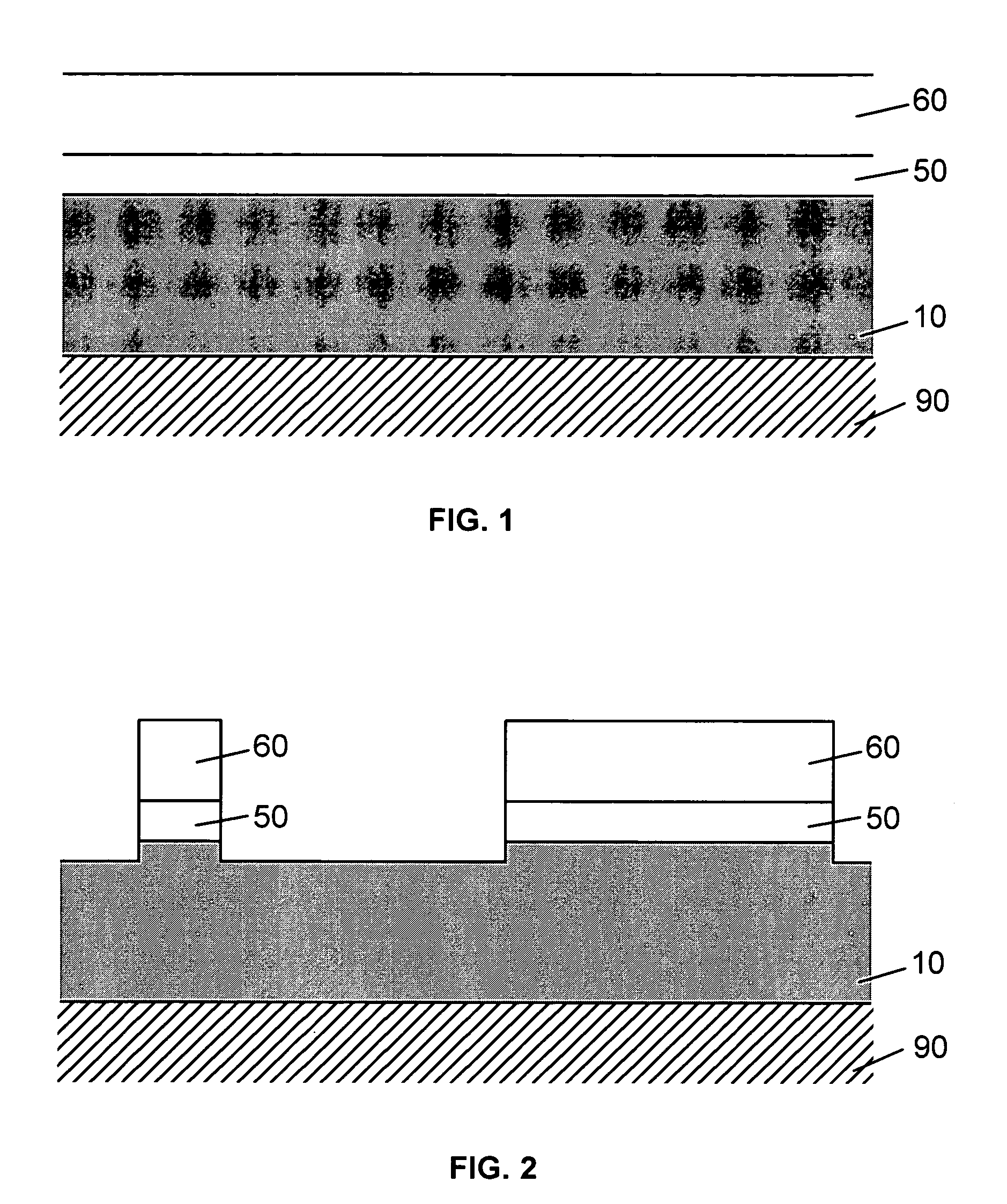
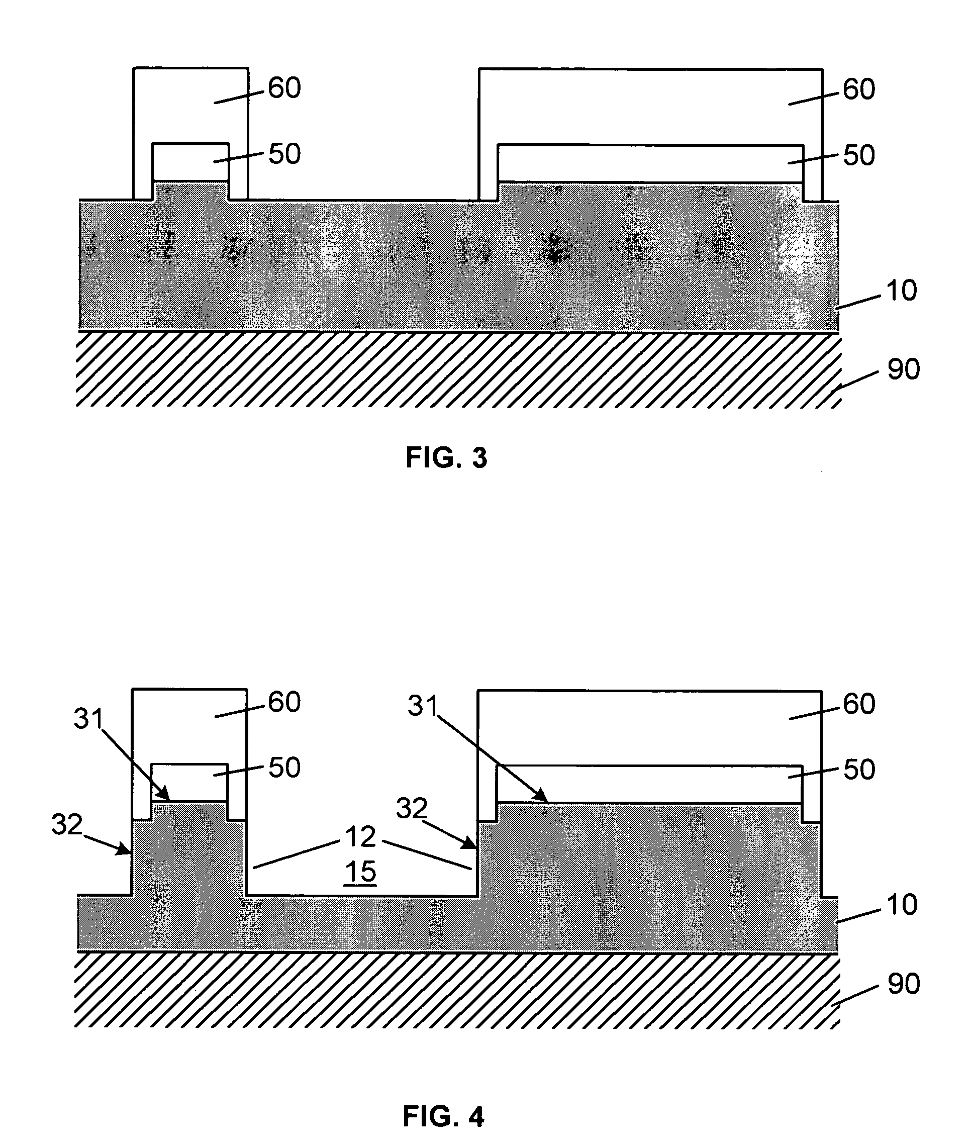
[0014]FIG. 1 shows a schematic cross sectional view of the initial stage of the fabrication of pedestals involving a semiconductor on insulator (SOI), usually Si on insulator wafer. It is understood that many phases of the description of pedestal fabrication refer to exemplary embodiments, and should not be interpreted in a restrictive manner, as one skilled in the art would recognize alternative paths of fabrication.

[0015]Providing a wafer is the starting point of the device fabrication process. The wafer may be a bulk Si wafer, a Si wafer with a Si based material layer on the surface, or a semiconductor on insulator (SOI) wafer. The figures depict a representative embodiment using a SOI wafer with the understanding that the depiction could equally well show a bulk wafer. In FIG. 1 a Si based material member 10, is a layer of an SOI wafer on top of a buried insulating layer 90. In alternative embodiments where the member 10 is a bulk wafer, the insulator 90 would not be present. Fo...


PUM


Abstract

A method of fabrication and a field effect device structure are presented that reduce source / drain capacitance and allow for device body contact. A Si based material pedestal is produced, the top surface and the sidewalls of which are oriented in a way to be substantially parallel with selected crystallographic planes of the pedestal and of a supporting member. The pedestal is wet etched with an anisotropic solution containing ammonium hydroxide. The sidewalls of the pedestal become faceted forming a segment in the pedestal with a reduced cross section. The dopant concentration in the reduced cross section segment is chosen to be sufficiently high for it to provide for electrical continuity through the pedestal.

Description

FIELD OF THE INVENTION[0001]The present invention relates to devices used in integrated circuits and their manufacturing. More particularly, the present invention relates to a field effect device fabrication process which improves device performance, and relates to the resulting device structure.BACKGROUND OF THE INVENTION[0002]Today's integrated circuits include a vast number of devices. Smaller devices and shrinking ground rules are the key to enhance performance and to improve reliability. As FET (Field Effect Transistor) devices are being scaled down, the technology becomes more complex, and changes in device structures and new fabrication methods are needed to maintain the expected performance enhancement from one generation of devices to the next. The mainstay material of microelectronics is silicon (Si), or more broadly, Si based materials. One such Si based material of importance for microelectronics is the silicon-germanium (SiGe) alloy.[0003]There is great difficulty in ma...

Claims


Application Information

Patent Timeline
Patent Type & Authority Patents(United States)
IPC IPC(8): H01L21/336
CPCH01L21/30608H01L21/84H01L27/1203H01L29/785H01L29/66772H01L29/045H01L29/66818
Inventor LI, YUJUNSETTLEMYER, JR., KENNETH T.BEINTNER, JOCHEN
Owner INT BUSINESS MASCH CORP
Why Eureka
Try Eureka