Nitride crystal, nitride crystal substrate, epilayer-containing nitride crystal substrate, semiconductor device and method of manufacturing the same

a technology of nitride crystal substrate and nitride crystal, which is applied in the direction of semiconductor/solid-state device testing/measurement, after-treatment details, instruments, etc., can solve the problems of difficult surface smoothing processing of nitride, affecting the performance of the semiconductor device including nitride, and difficult distortion removal processing after smoothing processing. achieve the effect of direct and reliable evaluation

Active Publication Date: 2008-08-26
SUMITOMO ELECTRIC IND LTD
View PDF7 Cites 41 Cited by
  • Summary
  • Abstract
  • Description
  • Claims
  • Application Information

AI Technical Summary

Benefits of technology

[0025]The invention can provide the nitride crystal having a crystal surface layer that is evaluated directly and reliably without breaking the crystal so that it can be used in a preferred fashion as a substrate for epitaxial crystal growth when producing a semiconductor device as well as the nitride crystal substrate, the epilayer-containing nitride crystal substrate, the semiconductor device and the method of manufacturing the same.

Problems solved by technology

Crystal quality of the epitaxially grown nitride semiconductor layer is affected by a state of a surface layer of the substrate used for the epitaxial growth, and this quality affects performance of the semiconductor device including the nitride semiconductor layer.
Among various compound semiconductors, gallium-nitride-based semiconductors are relatively hard so that the surface smoothing processing thereof is not easy, and the distortion removal processing after the smoothing processing is not easy.
However, the processing rate of the CMP processing is low, and causes problems in cost and productivity.
Further, the dry etching causes a problem in surface roughness.
The finishing method of the Si substrate using the CMP as well as the polishing agent for the method are not suitable for the hard nitride semiconductor substrate, and lower the removal speed of the surface layer.
In particular, GaN is chemically suitable, and is relatively resistant to the wet etching so that the CMP processing is not easy.
Although the dry etching can remove the nitride semiconductor surface, it does not have an effect of flattening the surface in a horizontal direction so that the surface smoothing effect cannot be achieved.
However, the crystal quality of the surface layer that is required at the substrate surface is not clear.
Thus, the distortions at the surface layer of the crystal have conventionally been evaluated by a breaking test that breaks the crystal, and therefore such problems occur that correction cannot be performed after the evaluation even when the result of evaluation was insufficient, and that the evaluation cannot be effected on the product in itself.
Under the present circumstances, there is no index for nondestructively evaluating the crystallinity of the surface layer at the finished substrate surface, and it is difficult to define quantitatively the crystal quality of the surface layer.

Method used


Image

  • Nitride crystal, nitride crystal substrate, epilayer-containing nitride crystal substrate, semiconductor device and method of manufacturing the same
  • Nitride crystal, nitride crystal substrate, epilayer-containing nitride crystal substrate, semiconductor device and method of manufacturing the same
  • Nitride crystal, nitride crystal substrate, epilayer-containing nitride crystal substrate, semiconductor device and method of manufacturing the same

Examples


first embodiment

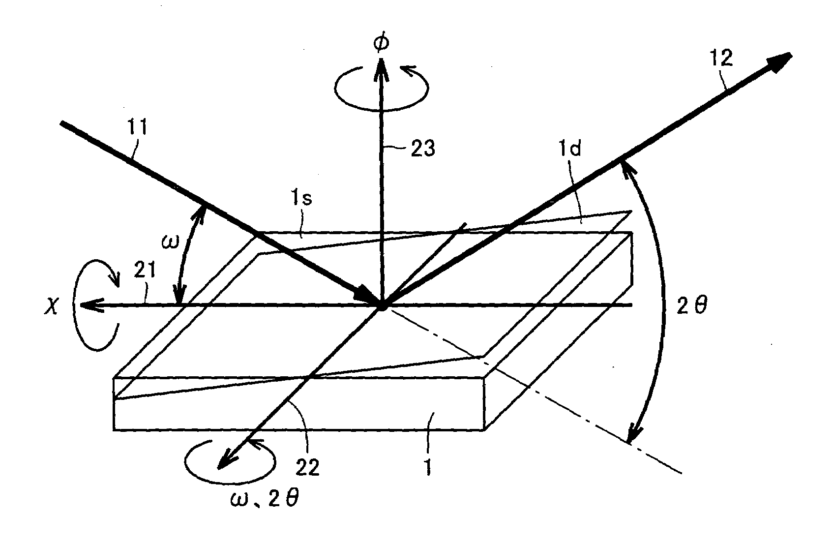
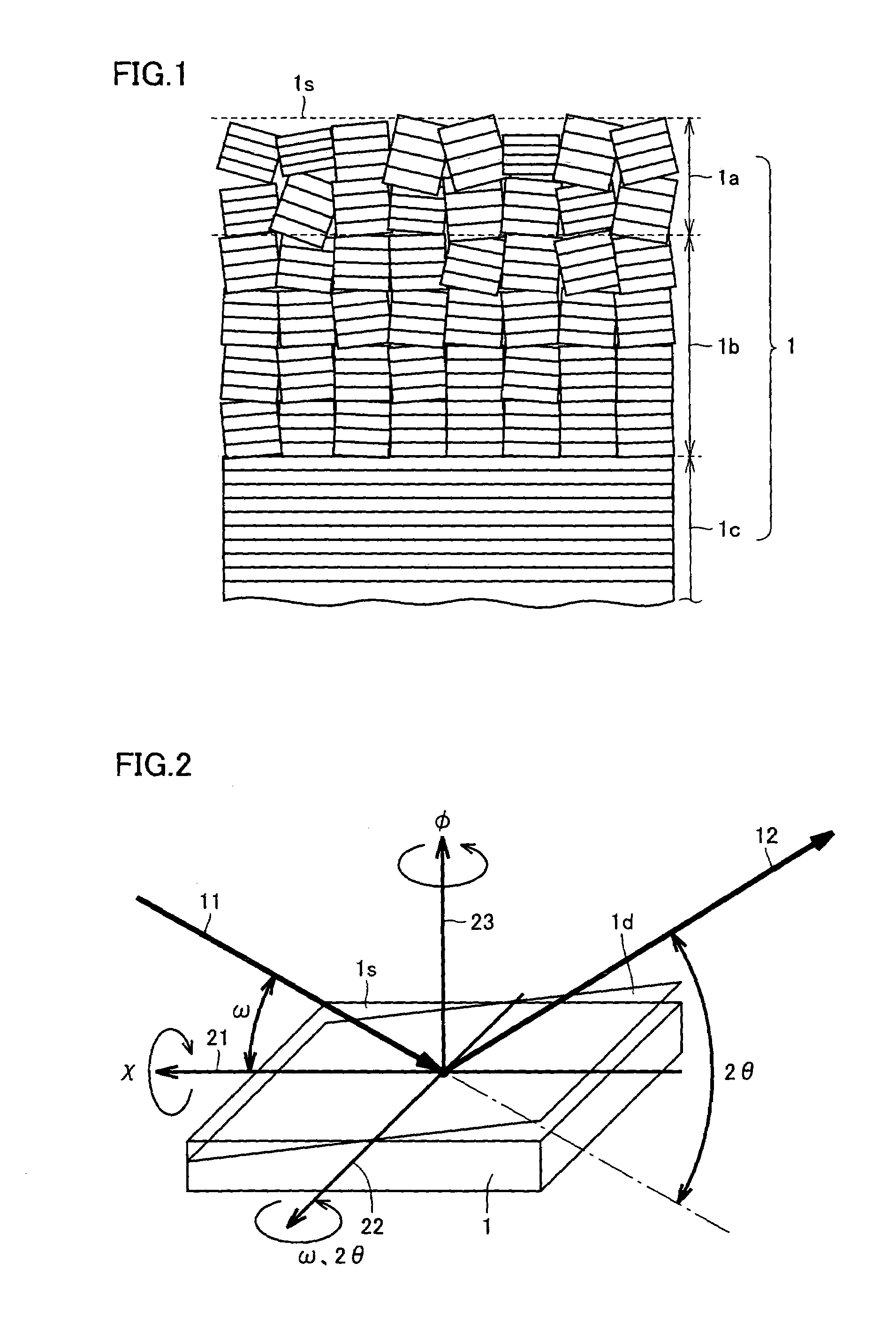
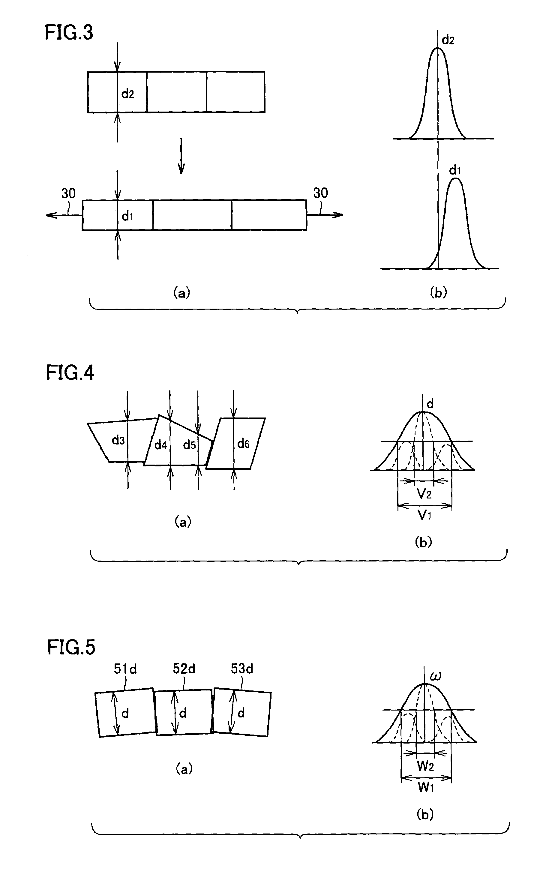
[0043]A nitride crystal of this embodiment is characterized in that, in connection with plane spacing of arbitrary specific parallel crystal lattice planes of the crystal obtained from X-ray diffraction measurement performed with variation of X-ray penetration depth from a surface of the crystal while X-ray diffraction conditions of the specific parallel crystal lattice planes are satisfied, a uniform distortion at a surface layer of the crystal represented by a value of |d1−d2| / d2 obtained from a plane spacing d1 at the X-ray penetration depth of 0.3 μm and a plane spacing d2 at the X-ray penetration depth of 5 μm is equal to or lower than 2.1×10⁻³.

[0044]Referring to FIG. 1, the X-ray penetration depth of 0.3 μm corresponds to a distance from the surface of the nitride crystal to an inside of crystal surface layer 1a, and the X-ray penetration depth of 5 μm corresponds to a distance from the surface of the nitride crystal to an inside of crystal inner layer 1c. Referring to FIG. 3(...

second embodiment

[0047]A nitride crystal of this embodiment is characterized in that, on a diffraction intensity profile of arbitrary specific parallel crystal lattice planes of the crystal obtained from X-ray diffraction measurement performed with variation of X-ray penetration depth from a surface of the crystal while X-ray diffraction conditions of the specific parallel crystal lattice planes are satisfied, an irregular distortion at a surface layer of the crystal represented by a value of |v1−v2| obtained from a half value width v1 of a diffraction intensity peak at the X-ray penetration depth of 0.3 μm and a half value width v2 of the diffraction intensity peak at the X-ray penetration depth of 5 μm is equal to or lower than 150 arcsec.

[0048]Referring to FIG. 1, the X-ray penetration depth of 0.3 μm corresponds to a distance from the surface of the nitride crystal to an inside of crystal surface layer 1a, and the X-ray penetration depth of 5 μm corresponds to a distance from the surface of the ...

third embodiment

[0051]A nitride crystal of this embodiment is characterized in that, on a rocking curve measured by varying an X-ray penetration depth from a crystal surface in connection with X-ray diffraction of arbitrary specific parallel crystal lattice planes of the crystal, a plane orientation deviation of the specific parallel crystal lattice planes represented by a value of |w1−w2| obtained from a half value width w1 of a diffraction intensity peak at the X-ray penetration depth of 0.3 μm and a half value width w2 of the diffraction intensity peak at the X-ray penetration depth of 5 μm is equal to or lower than 400 arcsec.

[0052]Referring to FIG. 1, the X-ray penetration depth of 0.3 μm corresponds to a distance from the surface of the nitride crystal to an inside of crystal surface layer 1a, and the X-ray penetration depth of 5 μm corresponds to a distance from the surface of the nitride crystal to an inside of crystal inner layer 1c. Referring to FIG. 5(a), half value width w2 at the X-ray...


PUM

PropertyMeasurementUnit
surface roughnessaaaaaaaaaa
RMS surface roughnessaaaaaaaaaa
surface roughness Ryaaaaaaaaaa

Abstract

A nitride crystal is characterized in that, in connection with plane spacing of arbitrary specific parallel crystal lattice planes of the nitride crystal obtained from X-ray diffraction measurement performed with variation of X-ray penetration depth from a surface of the crystal while X-ray diffraction conditions of the specific parallel crystal lattice planes are satisfied, a uniform distortion at a surface layer of the crystal represented by a value of |d1−d2| / d2 obtained from the plane spacing d1 at the X-ray penetration depth of 0.3 μm and the plane spacing d2 at the X-ray penetration depth of 5 μm is equal to or lower than 2.1×10⁻³. The above configuration provides the nitride crystal having a crystal surface layer that is evaluated directly and reliably without breaking the crystal so that it can be used in a preferred fashion as a substrate for a semiconductor device as well as the nitride crystal substrate, an epilayer-containing nitride crystal substrate, a semiconductor device and a method of manufacturing the same.

Description

[0001]This application claims benefit to of 60 / 688,674 Jun. 8, 2005.BACKGROUND OF THE INVENTION[0002]1. Field of the Invention[0003]The present invention relates to a nitride crystal, a nitride crystal substrate, an epilayer-containing nitride crystal substrate, a semiconductor device and a method of manufacturing the same, and particularly to a nitride crystal that can be preferably used as a substrate for growing an epitaxial crystal when producing a semiconductor device.[0004]2. Description of the Background Art[0005]As is well known, various devices using nitride semiconductor crystals have been produced in recent years, and nitride semiconductor light emitting devices have been produced as a typical example of such semiconductor devices.[0006]Generally, in a process of manufacturing a nitride semiconductor device, a plurality of nitride semiconductor layers are epitaxially grown on a substrate. Crystal quality of the epitaxially grown nitride semiconductor layer is affected by ...

Claims


Application Information

Patent Timeline
Patent Type & Authority Patents(United States)
IPC IPC(8): C30B25/12H01L33/06G01N23/20H01L21/66H01L33/32
CPCC30B29/403C30B33/00H01L29/045C30B29/38H01L29/04H01L29/2003Y10T428/2978C30B25/186C30B25/20C30B29/406C30B33/10G01B15/08G01N23/207G01N2223/602G01N2223/634H01L21/02389H01L21/02433H01L21/0254H01L22/12
Inventor ISHIBASHI, KEIJIKAJI, TOKIKONAKAHATA, SEIJINISHIURA, TAKAYUKI
Owner SUMITOMO ELECTRIC IND LTD
Why Eureka
Try Eureka