Integrated electrostatic inductive coupling for plasma processing

a plasma processing and electrostatic inductive coupling technology, applied in the direction of coatings, electric discharge lamps, electric lighting sources, etc., can solve the problems of chamber contamination, sputtering of these surfaces, and inability to allow real current to flow from the electrode to the rf generator, etc., to achieve high efficiency and reduce costs.

Inactive Publication Date: 2008-09-23
TOKYO ELECTRON LTD
View PDF14 Cites 14 Cited by
  • Summary
  • Abstract
  • Description
  • Claims
  • Application Information

AI Technical Summary

Benefits of technology

[0013]An objective of the present invention is to provide a plasma source for utilization in a plasma process, such as plasma etching, plasma deposition or plasma cleaning, that is uniform across the surface of the substrate being processed. Another objective of the invention is to provide a compact plasma source that can be used either as primary plasma source or as complementary source to a primary ICP source. A further objective of the invention is to provide a highly effective plasma source for a simplified reduced cost chamber.
[0017]According to certain principles of the present invention, the integrated wafer chuck and active peripheral ionization source is provided. With the source, plasma is generated in the vicinity of the wafer where it will affect immediately the plasma distribution above the wafer. Because of the close proximity of the source to the wafer, the source does not require a large RF power supply. The source may be used as a secondary or complementary source with which plasma is generated that compensates for non-uniformity generated by a primary ICP source. The source of the present invention generates a higher density plasma that diffuses into a low-density capacitively-coupled plasma above the wafer. With the present invention, RF hardware can be reduced in size and power. The source may be used as a single integrated plasma source sufficient to process wafers placed on the pedestal, which may be, for example, an electrostatic chuck (ESC).
[0018]The present invention is based, in part, on the principles that etch uniformity at a wafer is affected by plasma density distribution and by ion energy, and that to achieve uniform etching, uniformly distributed plasma parameters should be provided. It has been found that it is not sufficient to reduce the loss to the walls only in a passive way, and that the most effective way to reduce loss to the walls is to generate an active plasma in the depleted region around the wafer. Plasma density above the wafer is most easily affected by plasma generation in the vicinity of the wafer. This is done by using ICP, which leads to high-density plasma generation. This approach does not require oversized RF power supplies. The present invention utilizes existing RF generators to bias a wafer pedestal. A center-peaked plasma distribution that is generated by the remote primary ICP source may be compensated for at the wafer edge by peripheral plasma generation from a secondary high-density plasma source according to the present invention.

Problems solved by technology

Capacitively-coupled plasma sources include “planar diode” or “parallel plate” systems, in which a surface to be etched is placed on one electrode that is coupled to an RF generator through a blocking capacitor, which does not allow real current to flow from the electrode to the RF generator.
Capacitively-coupled sources have widespread use in semiconductor plasma processing, but have some problems and limitations.
In symmetrical systems, both electrodes can be subjected to high-energy ion bombardment, including energetic ion bombardment of walls and fixtures causing sputtering of these surfaces and chamber contamination.
Non-uniform plasma caused by large losses of electrons and ions to the chamber walls causes nonuniform etch rates to result.
Optimal geometry at low pressure has been cylindrical geometry, which is not adaptable to 300 mm single wafer semiconductor equipment manufacturing.
A common drawback of the above-described systems is an inability to independently control ion energy and ion flux at a fixed pressure and RF frequency.
Increasing the source power results in both an increase in the ion flux and a decrease in the ion energy.
Unfortunately, the magnetic confinement ring often produces the well-known cusp effect on the peripheral surface of the wafer due to the magnetic field of the confinement ring.
Still, the sidewall effect is not removed definitively from the wafer.
For current 300 mm size wafers, all these components represent large and expensive consumable parts, increased complexity, resulting in high cost of operation (COO) and significantly high overall cost of the machine.
Furthermore, producing uniformly distributed plasma over a wafer may have the undesirable effect of reducing plasma density.
Hence, the etch or deposition process may take longer to complete in a uniformly distributed plasma environment.

Method used


Image

  • Integrated electrostatic inductive coupling for plasma processing
  • Integrated electrostatic inductive coupling for plasma processing
  • Integrated electrostatic inductive coupling for plasma processing

Examples


Embodiment Construction

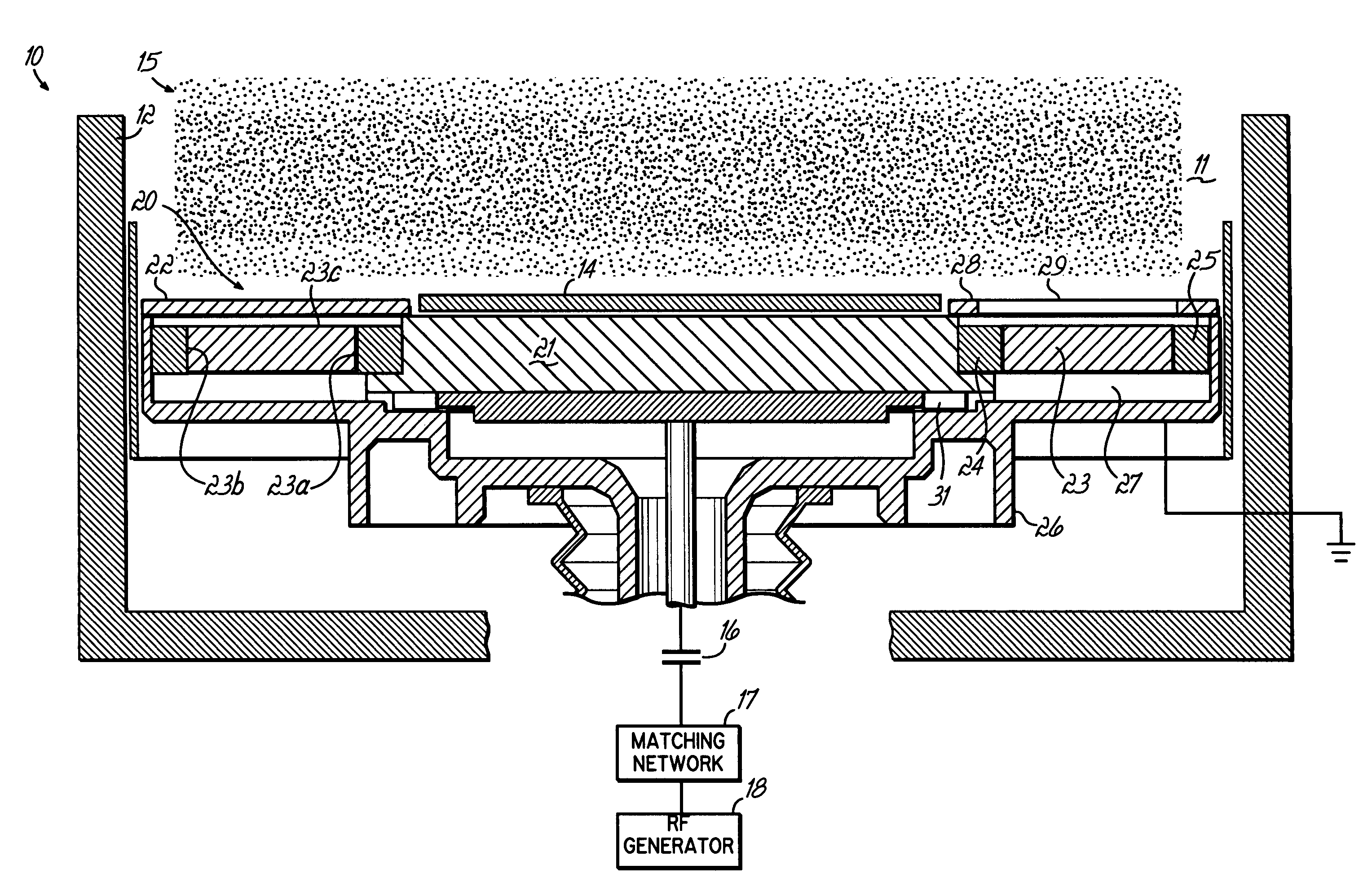
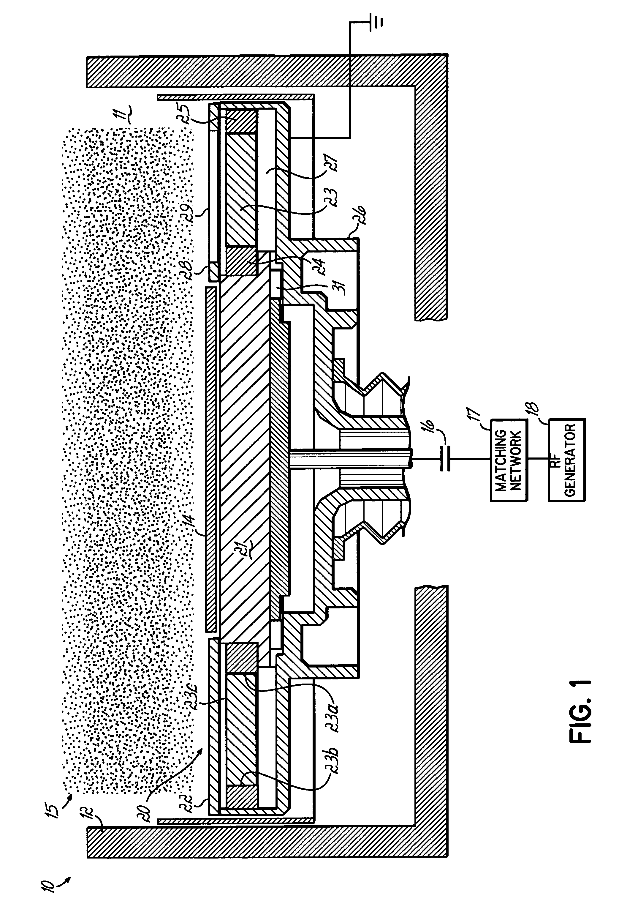
[0032]As illustrated in FIG. 1, according to one embodiment of the invention, a plasma processing apparatus 10 includes a vacuum processing chamber 11 enclosed in a chamber wall 12. An integrated, electrostatic inductively-coupled device or wafer support (i-ESIC) 20 is mounted in the chamber 11 to support individual wafers 14 thereon for processing by a plasma 15 maintained within the vacuum chamber 11.

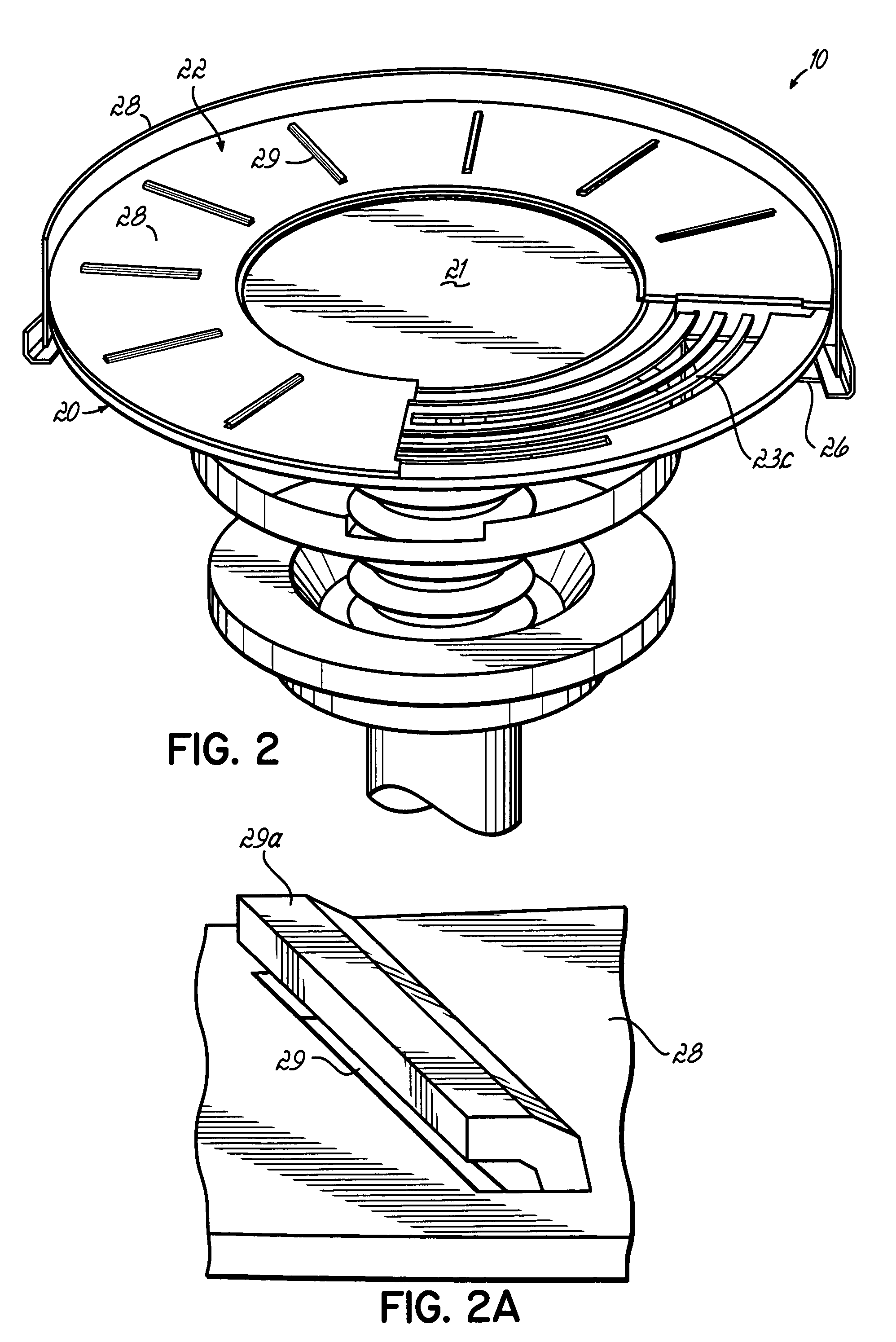
[0033]Referring to FIGS. 1 and 2, the wafer support 20 has two integrated main components or portions: a capacitive-coupling component 21, which provides a capacitively-coupled RF path to a plasma 15, and an inductively-coupled component 22, which provides an inductively-coupled RF path to the plasma 15. The capacitively-coupled component 21 is a central substrate support portion, typically an electrostatic chuck (ESC), which holds individual wafers to the support 20 during processing. The chuck of the central portion 21 also provides control of the energy of ions from the plasma by c...


PUM

PropertyMeasurementUnit
pressuresaaaaaaaaaa
diametersaaaaaaaaaa
slot widthaaaaaaaaaa

Abstract

An integrated electrostatic inductively-coupled (i-ESIC) device is provided for plasma processing that may be used as a primary or secondary source for generating a plasma to prepare substrates for, and to process substrates by applying, dielectric and conductive coatings. The i-ESIC device is practical for processing advanced semiconductor devices and integrated circuits that require uniform and dense plasma. The invention may be embodied in an apparatus that contains a substrate support, typically including an electrostatic chuck, that controls ion energy by capacitively coupling RF power to the plasma and generating voltage bias on the wafer relative to the plasma potential. An integrated inductive coupling element is provided at the perimeter of the substrate support that increases plasma density at the perimeter of the wafer, compensating for the radial loss of charged particles toward chamber walls, to produce uniform plasma density above the processed wafer. An annular slotted shield protects the inductive coupling element from the plasma and provides conditions for effective inductive coupling of RF power into the plasma, such as eliminating capacitive coupling from the element to the plasma and unwanted sputtering of the element. The i-ESIC device has a capacitive coupling zone in its center where wafers are placed and an inductive coupling zone at the perimeter of the wafer coupled to a matching network and RF generator. Both zones together with plasma create a resonant circuit.

Description

[0001]This invention relates to high density plasma generating devices, systems and processes, particularly for the manufacture of semiconductor wafers. This invention particularly relates to the high density inductively coupled plasma sources with slotted deposition baffles and RF biased wafer supports used in semiconductor processing.BACKGROUND OF THE INVENTION[0002]There are two principal groups of the plasma sources: capacitively-coupled plasma sources, which utilize RF electric field coupling to the plasma, and inductively coupled plasma (ICP) sources, which utilizing RF magnetic field coupling to the plasma.[0003]Capacitively-coupled plasma sources include “planar diode” or “parallel plate” systems, in which a surface to be etched is placed on one electrode that is coupled to an RF generator through a blocking capacitor, which does not allow real current to flow from the electrode to the RF generator. This forces the plasma to find a condition in which the electron current rea...

Claims


Application Information

Patent Timeline
Patent Type & Authority Patents(United States)
IPC IPC(8): C23C16/00C23F1/00H01L21/306H01J37/32
CPCH01J37/32174H01J37/321
Inventor BRCKA, JOZEF
Owner TOKYO ELECTRON LTD
Why Eureka
Try Eureka